74HC173
74HC173 is Quad D-Type Flip-Flop manufactured by Texas Instruments.
CD54HC173, CD74HC173, CD54HCT173, CD74HCT173
SCHS158F
- NOVEMBER 1998
- REVISED MARCH 2022
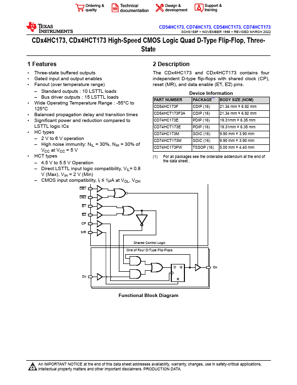
CDx4HC173, CDx4HCT173 High-Speed CMOS Logic Quad D-Type Flip-Flop, ThreeState
1 Features
- Three-state buffered outputs
- Gated input and output enables
- Fanout (over temperature range)
- Standard outputs : 10 LSTTL loads
- Bus driver outputs : 15 LSTTL loads
- Wide Operating Temperature Range : -55°C to 125°C
- Balanced propagation delay and transition times
- Significant power and reduction pared to LSTTL logic ICs
- HC types
- 2 V to 6 V operation
- High noise immunity: NIL = 30%, NIH = 30% of
VCC at VCC = 5 V
- HCT types
- 4.5 V to 5.5 V Operation
- Direct LSTTL input logic patibility,...