Texas Instruments ADC10040
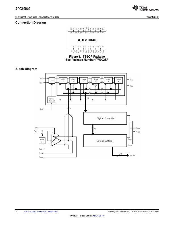
The ADC10040 is a monolithic CMOS analog-todigital converter capable of converting analog input signals into 10-bit digital words at 40 Megasamples per second (MSPS). This converter uses a differential, pipeline architecture with digital error correction and an on-chip sample-and-hold circuit to provide a complete conversion solution, and to minimize power consumption, while providing excellent dynamic performance. The Standby feature reduces power consumption to just 13.5 mW.| Part No. | ADC10040 |
|---|---|
| Datasheet | ADC10040 Download |
| Manufacturer |  Texas Instruments |
| Description | 10-Bit 40MSPS 3V 55.5mW A/D Converter |
| Buy | Stock & Price |
FEATURES
1●2 Single +3.0V Operation
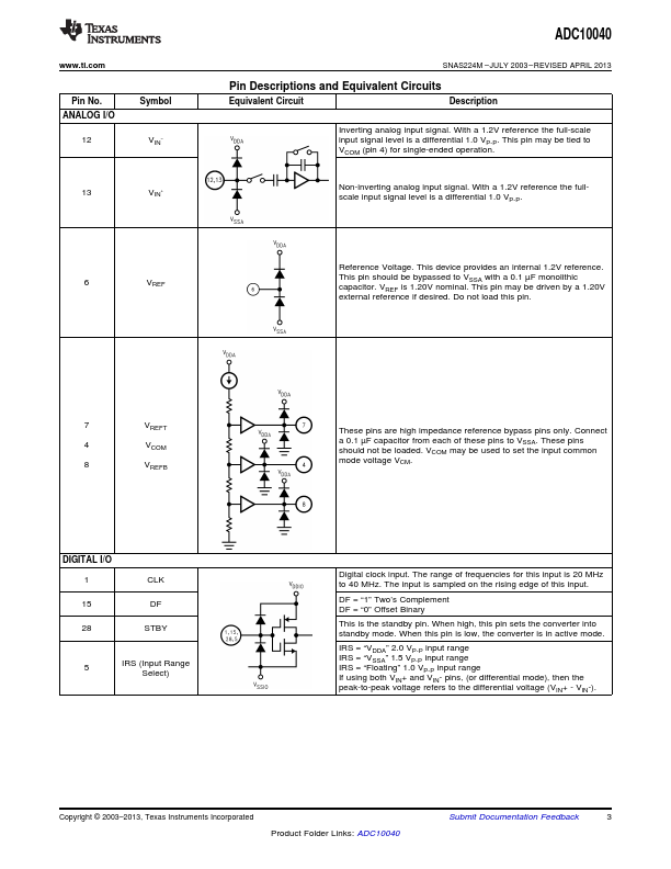
● Selectable 2.0 VP-P, 1.5 VP-P, or 1.0 VP-P full- scale input swing
● 400 MHz −3 dB Input Bandwidth
● Low Power Consumption
● Standby Mode
● On-Chip Reference and Sample-and-Hold Amplifier
● Offset Binary or Two’s Complement Data Format
● Separate Adjustable Output Driver Supply to Accommodate 2.5V and 3.3V Logic Families
● AEC-Q100 Grade 3 Qualified
● 28-Pin TSSOP Package KEY SPECIFICATIONS
● Resolution: 10 Bits
● Conversion Rate: 40 MSPS
● Full Power Bandwidth: 400 MHz
● DNL: ±0.3 LSB typ)
● SNR (fIN = 11 MHz): 59.6 dB (typ)
● SFDR (fIN = 11 MHz): -80 dB (typ)
● Power Consumption, 40 MHz: 55.5 mW
APPLICATIONS
● Ultrasound and Imaging● Instrumentation
● Cellular Base Stations/Communications Receivers
● Sonar/Radar
● xDSL
● Wireless Local Loops
● Data Acquisition Systems
● DSP Front Ends
DESCRIPTION
A unique sampleand-hold stage yields a full-power bandwidth of 400 MHz. Operating on a single 3.0V power supply, this device consumes just 55.5 mW at 40 MSPS, including the reference current.