Texas Instruments ADC3243
The ADC324x are a high-linearity, ultra-low power, dual-channel, 14-bit, 25-MSPS to 125-MSPS, analogto-digital converter (ADC) family. The devices are designed specifically to support demanding, high input frequency signals with large dynamic range requirements. The ADC324x family supports serial low-voltage differential signaling (LVDS) in order to reduce the number of interface lines, thus allowing for high system integration density.| Part No. | ADC3243 |
|---|---|
| Datasheet | ADC3243 Download |
| Manufacturer |  Texas Instruments |
| Description | Analog-to-Digital Converter |
| Buy | Stock & Price |
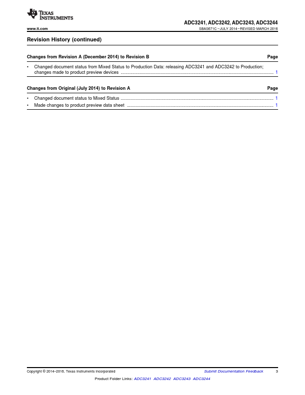
FEATURES
●1 Dual Channel● 14-Bit Resolution
● Single Supply: 1.8 V
● Serial LVDS Interface (SLVDS)
● Flexible Input Clock Buffer with Divide-by-1, -2, -4
● SNR = 72.4 dBFS, SFDR = 87 dBc at fIN = 70 MHz
● Ultra-Low Power Consumption: – 116 mW/Ch at 125 MSPS
● Channel Isolation: 105 dB
● Internal Dither and Chopper
● Support for Multi-Chip Synchronization
● Pin-to-Pin Compatible with 12-Bit Version
● Package: VQFN-48 (7 mm × 7 mm) 2
APPLICATIONS
● Multi-Carrier, Multi-Mode Cellular Base Stations● Radar and Smart Antenna Arrays
● Munitions Guidance
● Motor Control Feedback
● Network and Vector Analyzers
● Communications Test Equipment
● Nondestructive Testing
● Microwave Receivers
● Software-Defined Radios (SDRs)
● Quadrature and Diversity Radio Receivers
● Handheld Radio and Instrumentation 3
DESCRIPTION
An input clock divider allows more flexibility for system clock architecture design and the SYSREF input enables complete system synchronization. The serial LVDS interface is two-wire, where each ADC data are serialized and output over two LVDS pairs.