ADS9110
ADS9110 is 18-Bit 2-MSPS 15-mW SAR ADC manufactured by Texas Instruments.
Features
1 Features
- 1 Sample Rate: 2 MSPS
- No Latency Output
- Excellent DC and AC Performance:
- INL: ±0.5 LSB
- DNL: ±0.75 LSB
- SNR: 100 d B, THD:
- 118 d B
- Wide Input Range:
- Unipolar Differential Input Range: ±VREF
- VREF Input Range: 2.5 V to 5 V,
Independent of AVDD
- Low-Power Dissipation:
- 9 m W at 2 MSPS (AVDD Only)
- 15 m W at 2 MSPS (Total)
- Flexible Low-Power Modes Enable Power
Scaling with Throughput
- Enhanced-SPI (multi SPI™) Digital Interface
- JESD8-7A-pliant Digital I/O at 1.8-V DVDD
- Fully-Specified Over Extended Temperature
Range:
- 40°C to +125°C
- Small Footprint: 4-mm × 4-mm VQFN
2 Applications
- Test and Measurement
- Motor Control
- Medical Imaging
- High-Precision, High-Speed Industrial
3 Description
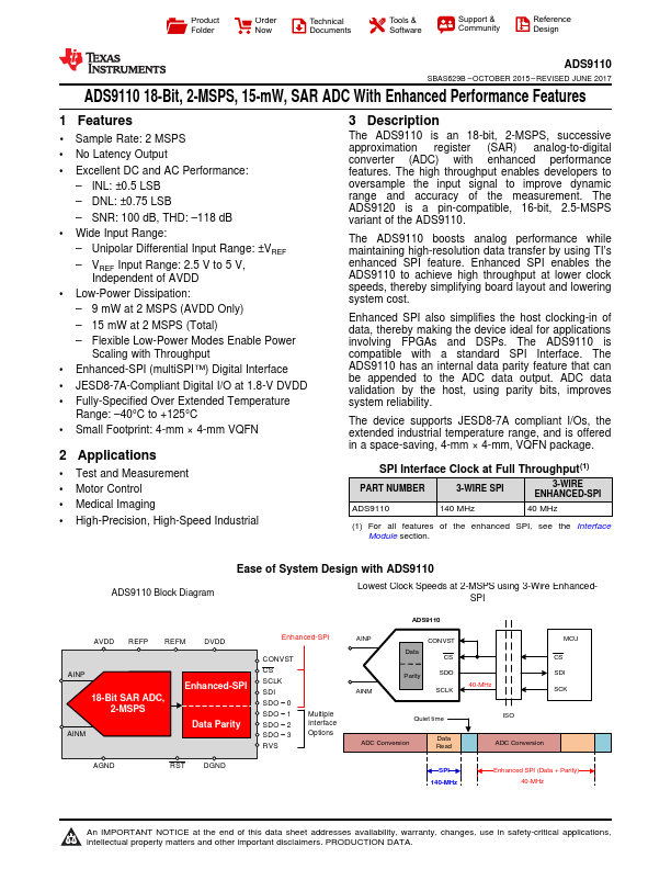
The ADS9110 is an 18-bit, 2-MSPS, successive approximation register (SAR) analog-to-digital converter (ADC) with enhanced performance features
. The high throughput enables developers to oversample the input signal to improve dynamic range and accuracy of the measurement. The ADS9120 is a pin-patible, 16-bit, 2.5-MSPS variant of the ADS9110.
The ADS9110 boosts analog performance while maintaining high-resolution data transfer by using TI’s enhanced SPI feature
. Enhanced SPI enables the ADS9110 to achieve high throughput at lower clock speeds, thereby simplifying board layout and lowering system cost.
Enhanced SPI also simplifies the host clocking-in of data, thereby making the device ideal for applications involving FPGAs and DSPs. The ADS9110 is patible with a standard SPI Interface. The ADS9110 has an internal data parity feature that can be appended to the ADC data output. ADC data validation by the host, using parity bits, improves system reliability.
The device supports JESD8-7A pliant I/Os, the extended industrial temperature range, and is offered in a space-saving, 4-mm × 4-mm, VQFN package.
SPI Interface Clock at Full Throughput(1)
PART NUMBER
3-WIRE SPI
3-WIRE...