Datasheet4U.com
🌙
CD74ACT297 Datasheet | Texas Instruments
Part:
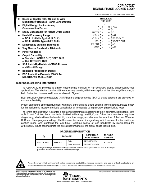
CD74ACT297
Description:
DIGITAL PHASE-LOCKED LOOP
Manufacturer:
Texas Instruments
Size:
396.54 KB
CD74ACT297 Datasheet (PDF) Download
Texas Instruments
CD74ACT297
Key Features
POST OFFICE BOX 655303 DALLAS, TEXAS 75265
POST OFFICE BOX 655303 DALLAS, TEXAS 75265
×
Close