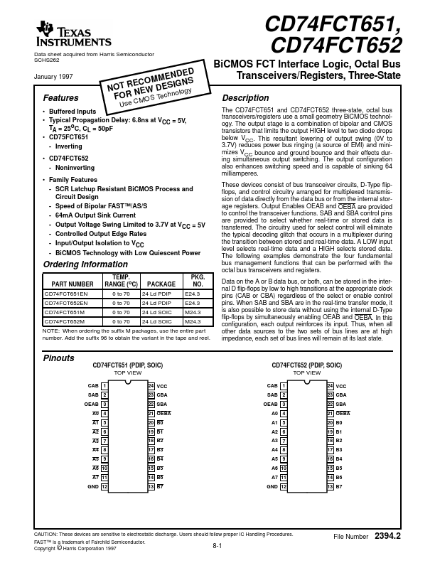
CD74FCT652
Features
- Buffered Inputs
NOFOUTs RRe ECNCMEOOWSMDTMe Ec Eh SNn Io GDlo NEg SDy
- Typical Propagation Delay: TA = 25o C, CL = 50p F
6.8ns at
=
5V,
Transceivers/Registers, Three-State
Description
The CD74FCT651 and CD74FCT652 three-state, octal bus transceivers/registers use a small geometry Bi CMOS technology. The output stage is a bination of bipolar and CMOS transistors that limits the output HIGH level to two diode drops
- CD75FCT651
- Inverting
- CD74FCT652 below VCC. This resultant lowering of output swing (0V to 3.7V) reduces power bus ringing (a source of EMI) and minimizes VCC bounce and ground bounce and their effects during simultaneous output switching. The output configuration
- Noninverting also enhances switching speed and is capable of sinking 64 milliamperes.
- Family Features
- SCR Latchup Resistant Bi CMOS Process and Circuit Design
These devices consist of bus transceiver circuits, D-Type flipflops, and control circuitry arranged for multiplexed transmission...