CDCLVD110
Overview
The CDCLVD110 clock driver distributes one pair of differential LVDS clock inputs (either CLK0 or CLK1) to 10 pairs of differential clock outputs (Q0, Q9) with minimum skew for clock distribution. The CDCLVD110 is specifically designed for driving 50-Ω transmission lines.
- Low-Output Skew <30 ps (Typical) for Clock-Distribution Applications
- Distributes One Differential Clock Input to 10 LVDS Differential Clock Outputs
- VCC range 2.5 V ±5%
- Typical Signaling Rate Capability of Up to
- 1 GHz
- Configurable Register (SI/CK) Individually Enables Disables Outputs, Selectable CLK0, CLK0 or CLK1, CLK1 Inputs
- Full Rail-to-Rail Common-Mode Input Range
- Receiver Input Threshold ±100 mV
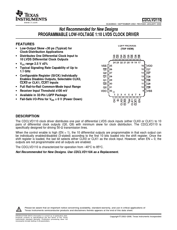
- Available in 32-Pin LQFP Package
- Fail-Safe I/O-Pins for VDD = 0 V (Power Down)