CDCM1802
Description
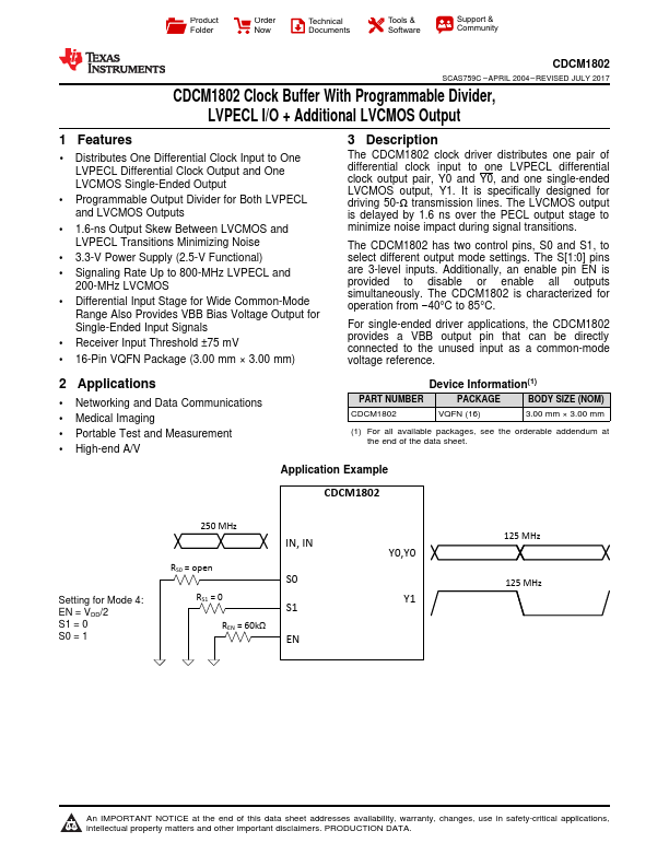
The CDCM1802 clock driver distributes one pair of differential clock input to one LVPECL differential clock output pair, Y0 and Y0, and one single-ended LVCMOS output, Y1.
Key Features
- 1 Distributes One Differential Clock Input to One LVPECL Differential Clock Output and One LVCMOS Single-Ended Output
- Programmable Output Divider for Both LVPECL and LVCMOS Outputs
- 1.6-ns Output Skew Between LVCMOS and LVPECL Transitions Minimizing Noise
- 3.3-V Power Supply (2.5-V Functional)
- Signaling Rate Up to 800-MHz LVPECL and
- Receiver Input Threshold ±75 mV
- 16-Pin VQFN Package (3.00 mm × 3.00 mm)
Applications
- Networking and Data munications