CSD18531Q5A Overview
Description
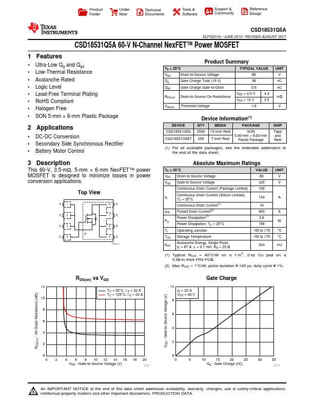
This 60-V, 3.5-mΩ, 5-mm × 6-mm NexFET™ power MOSFET is designed to minimize losses in power conversion applications. Top View S1 8D S2 7D S3 G4 D 6D 5D P0093-01 TA = 25°C VDS Drain-to-Source Voltage VGS Gate-to-Source Voltage Continuous Drain Current (Package Limited) VALUE 60 ±20 100 UNIT V V ID Continuous Drain Current (Silicon Limited), TC = 25°C Continuous Drain Current(1) IDM Pulsed Drain Current(2) Power Dissipation(1) PD Power Dissipation, TC = 25°C TJ Operating Junction Tstg Storage Temperature EAS Avalanche Energy, Single Pulse ID = 67 A, L = 0.1 mH, RG = 25 Ω 134 19 400 3.8 156 –55 to 175 –55 to 175 224 A A W °C °C mJ (1) Typical RθJA = 40°C/W on a 1-in2, 2-oz Cu pad on a 0.06-in thick FR4 PCB.
Key Features
- 1 Ultra-Low Qg and Qgd
- Avalanche Rated
- Lead-Free Terminal Plating
- RoHS Compliant
- Halogen Free
- SON 5-mm × 6-mm Plastic Package