Datasheet4U Logo Datasheet4U.com

DS90C365A - +3.3V Programmable LVDS Transmitter

General Description

The DS90C365A is a pin to pin compatible replacement for DS90C363, DS90C363A and DS90C365.

Key Features

  • 1.
  • 23 Pin-to-pin compatible to DS90C363, DS90C363A and DS90C365.
  • No special start-up sequence required between clock/data and /PD pins. Input signals (clock and data) can be applied either before or after the device is powered.
  • Support Spread Spectrum Clocking up to 100kHz frequency modulation & deviations of ±2.5% center spread or -5% down spread.
  • “Input Clock Detection” feature will pull all LVDS pairs to logic low when input clock is missing and when /PD p.

📥 Download Datasheet

Full PDF Text Transcription (Reference)

The following content is an automatically extracted verbatim text from the original manufacturer datasheet and is provided for reference purposes only.

View original datasheet text
DS90C365A www.ti.com SNLS181I – APRIL 2004 – REVISED APRIL 2013 
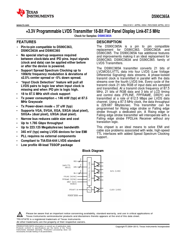
+3.3V Programmable LVDS Transmitter 18-Bit Flat Panel Display Link-87.5 MHz Check for Samples: DS90C365A FEATURES 1 •23 Pin-to-pin compatible to DS90C363, DS90C363A and DS90C365 • No special start-up sequence required between clock/data and /PD pins. Input signals (clock and data) can be applied either before or after the device is powered. • Support Spread Spectrum Clocking up to 100kHz frequency modulation & deviations of ±2.5% center spread or -5% down spread. • “Input Clock Detection” feature will pull all LVDS pairs to logic low when input clock is missing and when /PD pin is logic high. • 18 to 87.5 MHz shift clock support • Tx power consumption < 146 mW (typ) at 87.