Datasheet4U Logo Datasheet4U.com

DS90CF364 - +3.3V Programmable LVDS Transmitter

This page provides the datasheet information for the DS90CF364, a member of the DS90C363 +3.3V Programmable LVDS Transmitter family.

Datasheet Summary

Description

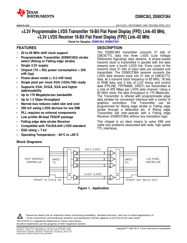
The DS90C363 transmitter converts 21 bits of CMOS/TTL data into three LVDS (Low Voltage Differential Signaling) data streams.

A phase-locked transmit clock is transmitted in parallel with the data streams over a fourth LVDS link.

Features

  • 1.
  • 23 20 to 65 MHz shift clock support.
  • Programmable Transmitter (DS90C363) strobe select (Rising or Falling edge strobe).
  • Single 3.3V supply.
  • Chipset (TX + RX) power consumption < 250 mW (typ).
  • Power-down mode (< 0.5 mW total).
  • Single pixel per clock XGA (1024×768) ready.
  • Supports VGA, SVGA, XGA and higher addressability.
  • Up to 170 Megabyte/sec bandwidth.
  • Up to 1.3 Gbps throughput.
  • Narrow bus reduces cable.

📥 Download Datasheet

Datasheet preview – DS90CF364

Datasheet Details

Part number DS90CF364
Manufacturer Texas Instruments
File Size 1.10 MB
Description +3.3V Programmable LVDS Transmitter
Datasheet download datasheet DS90CF364 Datasheet
Additional preview pages of the DS90CF364 datasheet.
Other Datasheets by Texas Instruments

Full PDF Text Transcription

Click to expand full text
DS90C363, DS90CF364 www.ti.com SNLS123C – SEPTEMBER 1999 – REVISED APRIL 2013 +3.3V Programmable LVDS Transmitter 18-Bit Flat Panel Display (FPD) Link–65 MHz, +3.3V LVDS Receiver 18-Bit Flat Panel Display (FPD) Link–65 MHz Check for Samples: DS90C363, DS90CF364 FEATURES 1 •23 20 to 65 MHz shift clock support • Programmable Transmitter (DS90C363) strobe select (Rising or Falling edge strobe) • Single 3.3V supply • Chipset (TX + RX) power consumption < 250 mW (typ) • Power-down mode (< 0.5 mW total) • Single pixel per clock XGA (1024×768) ready • Supports VGA, SVGA, XGA and higher addressability • Up to 170 Megabyte/sec bandwidth • Up to 1.
Published: |