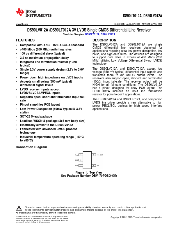
Datasheet4U Logo Datasheet4U.com

DS90LV012A - 3V LVDS Single CMOS Differential Line Receiver

Download the DS90LV012A datasheet PDF. This datasheet also covers the DS90LT012A variant, as both devices belong to the same 3v lvds single cmos differential line receiver family and are provided as variant models within a single manufacturer datasheet.

General Description

The DS90LV012A and DS90LT012A are single CMOS differential line receivers designed for applications requiring ultra low power dissipation, low noise, and high data rates.

Key Features

  • 1.
  • 2 Compatible with ANSI TIA/EIA-644-A Standard.
  • >400 Mbps (200 MHz) switching rates.
  • 100 ps differential skew (typical).
  • 3.5 ns maximum propagation delay.
  • Integrated line termination resistor (102Ω typical).
  • Single 3.3V power supply design (2.7V to 3.6V range).
  • Power down high impedance on LVDS inputs.
  • Accepts small swing (350 mV typical) differential signal levels.
  • LVDS receiver inputs accept LVDS/BLVDS/LVPECL inp.

📥 Download Datasheet

Note: The manufacturer provides a single datasheet file (DS90LT012A-etcTI.pdf) that lists specifications for multiple related part numbers.

Full PDF Text Transcription (Reference)

The following content is an automatically extracted verbatim text from the original manufacturer datasheet and is provided for reference purposes only.

View original datasheet text
DS90LT012A, DS90LV012A www.ti.com SNLS141D – AUGUST 2002 – REVISED APRIL 2013 DS90LV012A /DS90LT012A 3V LVDS Single CMOS Differential Line Receiver Check for Samples: DS90LT012A, DS90LV012A FEATURES 1 •2 Compatible with ANSI TIA/EIA-644-A Standard • >400 Mbps (200 MHz) switching rates • 100 ps differential skew (typical) • 3.5 ns maximum propagation delay • Integrated line termination resistor (102Ω typical) • Single 3.3V power supply design (2.7V to 3.6V range) • Power down high impedance on LVDS inputs • Accepts small swing (350 mV typical) differential signal levels • LVDS receiver inputs accept LVDS/BLVDS/LVPECL inputs • Supports open, short and terminated input fail- safe • Pinout simplifies PCB layout • Low Power Dissipation (10mW typical@ 3.