DS90LV049H
DS90LV049H is high temperature 3-V LVDS dual line driver and receiver pair manufactured by Texas Instruments.
Features
- 1 High Temperature +125°C Operating Range
- Up to 400-Mbps Switching Rates
- Flow-Through Pinout Simplifies PCB Layout
- 50-ps Typical Driver Channel-to-Channel Skew
- 50-ps Typical Receiver Channel-to-Channel Skew
- 3.3-V Single Power Supply Design
- TRI-STATE Output Control
- Internal Fail-Safe Biasing of Receiver Inputs
- Low Power Dissipation (70 m W at 3.3-V Static)
- High Impedance on LVDS Outputs on Power
Down
- Conforms to TIA/EIA-644-A LVDS Standard
- Available in Low Profile 16-Pin TSSOP Package
2 Applications
- Board-to-Board munication
- Test and Measurement
- Motor Drives
- LED Video Walls
- Wireless Infrastructure
- Tele Infrastructure
- Multi-Function Printers
- NIC Cards
- Rack Servers
- Ultrasound Scanners
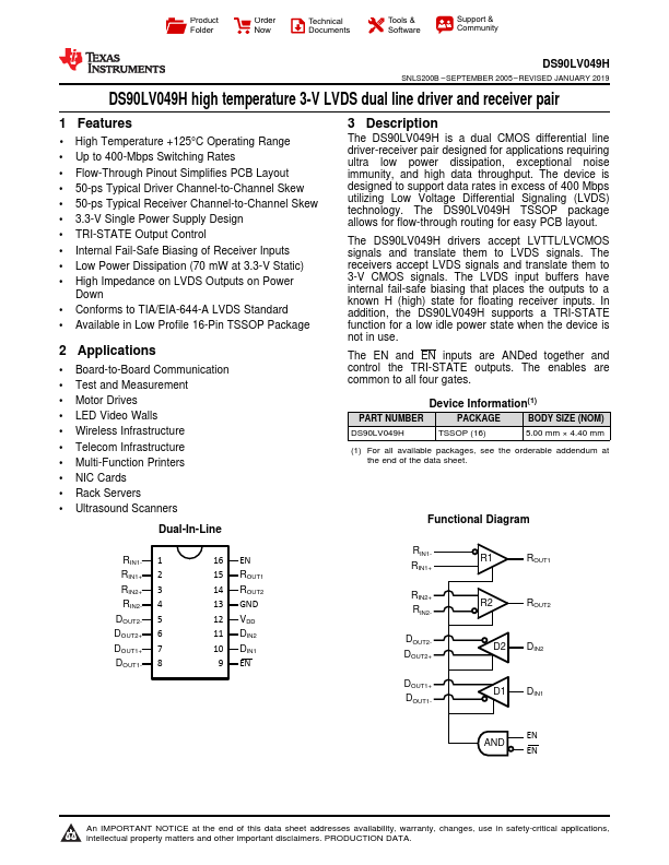
Dual-In-Line
3 Description
The DS90LV049H is a dual CMOS differential line driver-receiver pair designed for applications requiring ultra low power dissipation, exceptional noise immunity, and high data throughput. The device is designed to support data rates in excess of 400 Mbps utilizing Low Voltage Differential Signaling (LVDS) technology. The DS90LV049H TSSOP package allows for flow-through routing for easy PCB layout.
The DS90LV049H drivers accept LVTTL/LVCMOS signals and translate them to LVDS signals. The receivers accept LVDS signals and translate them to 3-V CMOS signals. The LVDS input buffers have internal fail-safe biasing that places the outputs to a known H (high) state for floating receiver inputs. In addition, the DS90LV049H supports a TRI-STATE function for a low idle power state when the device is not in use.
The EN and EN inputs are ANDed together and control the TRI-STATE outputs. The enables are mon to all four gates.
Device Information(1)
PART NUMBER
PACKAGE
BODY SIZE (NOM)
TSSOP (16)
5.00 mm × 4.40 mm
(1) For all available packages, see the orderable addendum at the end of the data sheet.
Functional Diagram
RIN1- 1 RIN1+ 2 RIN2+ 3 RIN2- 4 DOUT2- 5 DOUT2+ 6 DOUT1+ 7 DOUT1- 8
16...