DS90LV049H
DS90LV049H is High Temperature 3V LVDS Dual Line Driver and Receiver Pair manufactured by National Semiconductor.
Description
The DS90LV049H is a dual CMOS flow-through differential line driver-receiver pair designed for applications requiring ultra low power dissipation, exceptional noise immunity, and high data throughput. The device is designed to support data rates in excess of 400 Mbps utilizing Low Voltage Differential Signaling (LVDS) technology. The DS90LV049H drivers accept LVTTL/LVCMOS signals and translate them to LVDS signals. The receivers accept LVDS signals and translate them to 3 V CMOS signals. The LVDS input buffers have internal failsafe biasing that places the outputs to a known H (high) state for floating receiver inputs. In addition, the DS90LV049H supports a TRI-STATE function for a low idle power state when the device is not in use. The EN and EN inputs are ANDed together and control the TRI-STATE outputs. The enables are mon to all four gates.
Features n n n n n n n n n n n n High Temperature +125˚C Operating Range Up to 400 Mbps switching rates Flow-through pinout simplifies PCB layout 50 ps typical driver channel-to-channel skew 50 ps typical receiver channel-to-channel skew 3.3 V single power supply design TRI-STATE output control Internal fail-safe biasing of receiver inputs Low power dissipation (70 m W at 3.3 V static) High impedance on LVDS outputs on power down Conforms to TIA/EIA-644-A LVDS Standard Available in low profile 16 pin TSSOP package
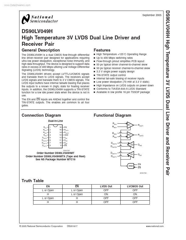
Connection Diagram
Dual-In-Line
Functional Diagram
Order Number DS90LV049HMT Order Number DS90LV049HMTX (Tape and Reel) See NS Package Number MTC16
Truth Table
EN L or Open H L or Open H EN L or Open L or Open H H LVDS Out OFF ON OFF OFF LVCMOS Out OFF ON OFF OFF
© 2005 National Semiconductor Corporation
DS201617
.national.
Absolute Maximum Ratings (Note 1)
If Military/Aerospace specified devices are required, please contact the National Semiconductor Sales Office/ Distributors for availability and specifications. Supply Voltage (VDD) LVCMOS Input Voltage (DIN)...