DS90LV049Q
DS90LV049Q is Automotive LVDS Dual Line Driver and Receiver Pair manufactured by Texas Instruments.
FEATURES
- 2 AECQ-100 Grade 1
- Up to 400 Mbps Switching Rates
- Flow-Through Pinout Simplifies PCB Layout
- 50 ps Typical Driver Channel-to-Channel Skew
- 50 ps Typical Receiver Channel-to-Channel
Skew
- 3.3 V Single Power Supply Design
- TRI-STATE Output Control
- Internal Fail-Safe Biasing of Receiver Inputs
- Low Power Dissipation (70 m W at 3.3 V Static)
- High Impedance on LVDS Outputs on Power
Down
- Conforms to TIA/EIA-644-A LVDS Standard
- Available in Low Profile 16 Pin TSSOP
Package
DESCRIPTION
The DS90LV049Q is a dual CMOS flow-through differential line driver-receiver pair designed for applications requiring ultra low power dissipation, exceptional noise immunity, and high data throughput. The device is designed to support data rates in excess of 400 Mbps utilizing Low Voltage Differential Signaling (LVDS) technology.
The DS90LV049Q drivers accept LVTTL/LVCMOS signals and translate them to LVDS signals. The receivers accept LVDS signals and translate them to 3 V CMOS signals. The LVDS input buffers have internal failsafe biasing that places the outputs to a known H (high) state for floating receiver inputs. In addition, the DS90LV049Q supports a TRI-STATE function for a low idle power state when the device is not in use.
The EN and EN inputs are ANDed together and control the TRI-STATE outputs. The enables are mon to all four gates.
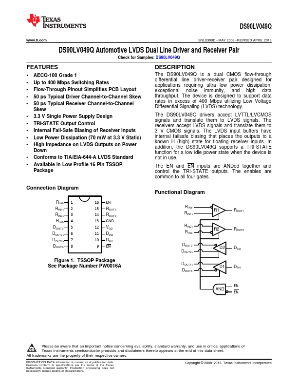
Connection Diagram
Functional Diagram
RIN1- 1 RIN1+ 2 RIN2+ 3 RIN2- 4 DOUT2- 5 DOUT2+ 6 DOUT1+ 7 DOUT1- 8
16 EN
15 ROUT1 14 ROUT2 13 GND
12 VDD 11 DIN2 10 DIN1
9 EN
Figure 1. TSSOP Package See Package Number PW0016A
RIN1RIN1+
RIN2+ RIN2-
DOUT2DOUT2+
DOUT1+ DOUT1-
R1
ROUT1
R2
ROUT2
D2
DIN2
D1...