SN54ABT827 Overview
Key Specifications
Output Type (varies by manufacturer): TTL
Description
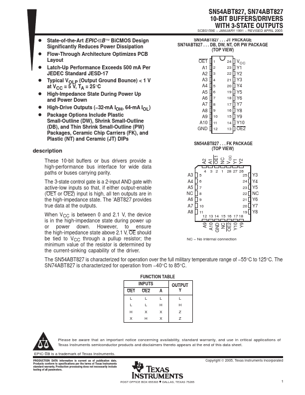
JT PACKAGE SN74ABT827. DB, DW, NT, OR PW PACKAGE (TOP VIEW) OE1 1 A1 2 A2 3 A3 4 A4 5 A5 6 A6 7 A7 8 A8 9 A9 10 A10 11 GND 12 24 VCC 23 Y1 22 Y2 21 Y3 20 Y4 19 Y5 18 Y6 17 Y7 16 Y8 15 Y9 14 Y10 13 OE2 SN54ABT827.