SN65LBC176A-EP
Overview
ąą D Controlled Baseline − One Assembly/Test Site, One Fabrication Site D Extended Temperature Performance of −40°C to 125°C and −55°C to 125°C D Enhanced Diminishing Manufacturing Sources (DMS) Suppo...
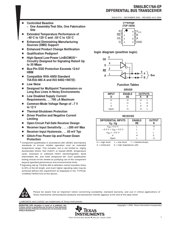
ąą D Controlled Baseline − One Assembly/Test Site, One Fabrication Site D Extended Temperature Performance of −40°C to 125°C and −55°C to 125°C D Enhanced Diminishing Manufacturing Sources (DMS) Suppo...