Datasheet4U Logo Datasheet4U.com

SN65LVDS250 - LVDS 4x4 CROSSPOINT SWITCH

General Description

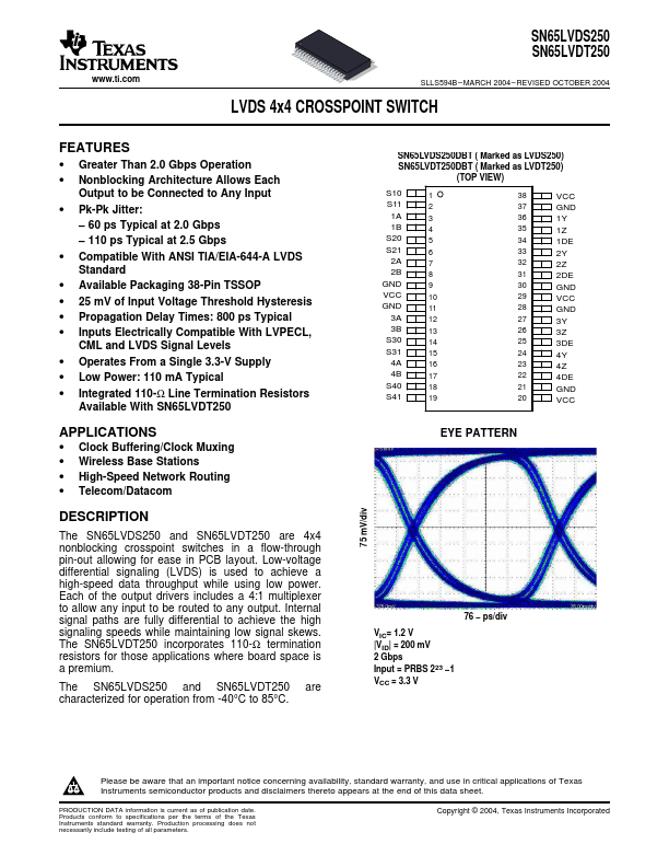
The SN65LVDS250 and SN65LVDT250 are 4x4 nonblocking crosspoint switches in a flow-through pin-out allowing for ease in PCB layout.

Low-voltage differential signaling (LVDS) is used to achieve a high-speed data throughput while using low power.

Key Features

  • Greater Than 2.0 Gbps Operation.
  • Nonblocking Architecture Allows Each Output to be Connected to Any Input.
  • Pk-Pk Jitter:.
  • 60 ps Typical at 2.0 Gbps.
  • 110 ps Typical at 2.5 Gbps.
  • Compatible With ANSI TIA/EIA-644-A LVDS Standard.
  • Available Packaging 38-Pin TSSOP.
  • 25 mV of Input Voltage Threshold Hysteresis.
  • Propagation Delay Times: 800 ps Typical.
  • Inputs Electrically Compatible With LVPECL, CML and LVDS Signa.

📥 Download Datasheet

Full PDF Text Transcription for SN65LVDS250 (Reference)

Note: Below is a high-fidelity text extraction (approx. 800 characters) for SN65LVDS250. For precise diagrams, and layout, please refer to the original PDF.

www.ti.com SN65LVDS250 SN65LVDT250 SLLS594B – MARCH 2004 – REVISED OCTOBER 2004 LVDS 4x4 CROSSPOINT SWITCH FEATURES • Greater Than 2.0 Gbps Operation • Nonblocking Archit...

View more extracted text
SWITCH FEATURES • Greater Than 2.0 Gbps Operation • Nonblocking Architecture Allows Each Output to be Connected to Any Input • Pk-Pk Jitter: – 60 ps Typical at 2.0 Gbps – 110 ps Typical at 2.5 Gbps • Compatible With ANSI TIA/EIA-644-A LVDS Standard • Available Packaging 38-Pin TSSOP • 25 mV of Input Voltage Threshold Hysteresis • Propagation Delay Times: 800 ps Typical • Inputs Electrically Compatible With LVPECL, CML and LVDS Signal Levels • Operates From a Single 3.