Datasheet4U Logo Datasheet4U.com

SN65LVP16 - 2.5-V/3.3-V OSCILLATOR GAIN STAGE/BUFFERS

This page provides the datasheet information for the SN65LVP16, a member of the SN65LVDS16 2.5-V/3.3-V OSCILLATOR GAIN STAGE/BUFFERS family.

Datasheet Summary

Description

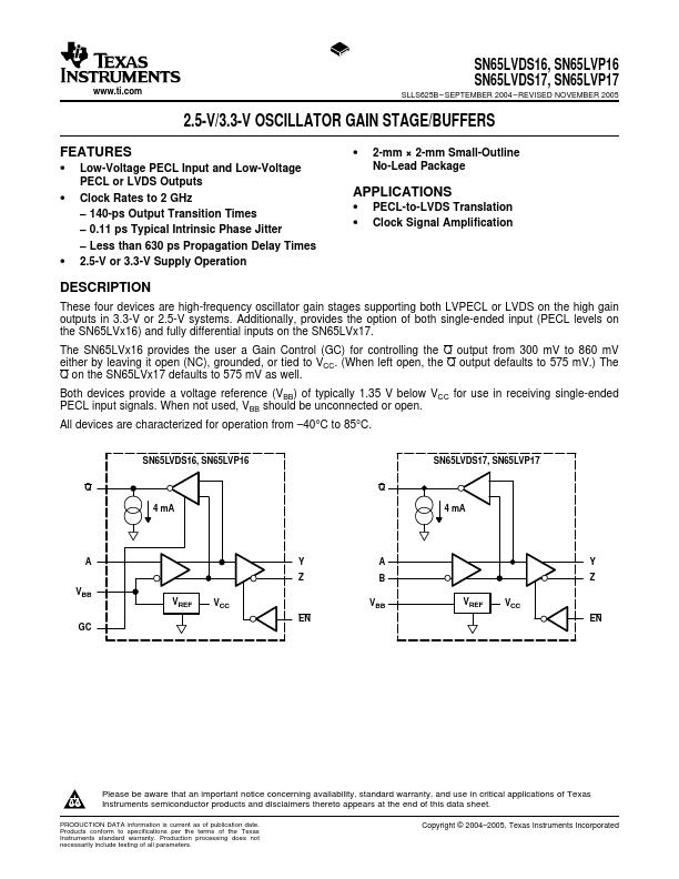
These four devices are high-frequency oscillator gain stages supporting both LVPECL or LVDS on the high gain outputs in 3.3-V or 2.5-V systems.

Additionally, provides the option of both single-ended input (PECL levels on the SN65LVx16) and fully differential inputs on the SN65LVx17.

Features

  • Low-Voltage PECL Input and Low-Voltage PECL or LVDS Outputs.
  • Clock Rates to 2 GHz.
  • 140-ps Output Transition Times.
  • 0.11 ps Typical Intrinsic Phase Jitter.
  • Less than 630 ps Propagation Delay Times.
  • 2.5-V or 3.3-V Supply Operation.
  • 2-mm × 2-mm Small-Outline No-Lead Package.

📥 Download Datasheet

Datasheet preview – SN65LVP16

Datasheet Details

Part number SN65LVP16
Manufacturer Texas Instruments
File Size 883.38 KB
Description 2.5-V/3.3-V OSCILLATOR GAIN STAGE/BUFFERS
Datasheet download datasheet SN65LVP16 Datasheet
Additional preview pages of the SN65LVP16 datasheet.
Other Datasheets by Texas Instruments

Full PDF Text Transcription

Click to expand full text
www.ti.com SN65LVDS16, SN65LVP16 SN65LVDS17, SN65LVP17 SLLS625B – SEPTEMBER 2004 – REVISED NOVEMBER 2005 2.5-V/3.3-V OSCILLATOR GAIN STAGE/BUFFERS FEATURES • Low-Voltage PECL Input and Low-Voltage PECL or LVDS Outputs • Clock Rates to 2 GHz – 140-ps Output Transition Times – 0.11 ps Typical Intrinsic Phase Jitter – Less than 630 ps Propagation Delay Times • 2.5-V or 3.3-V Supply Operation • 2-mm × 2-mm Small-Outline No-Lead Package APPLICATIONS • PECL-to-LVDS Translation • Clock Signal Amplification DESCRIPTION These four devices are high-frequency oscillator gain stages supporting both LVPECL or LVDS on the high gain outputs in 3.3-V or 2.5-V systems.
Published: |