SN65LVP17
Description
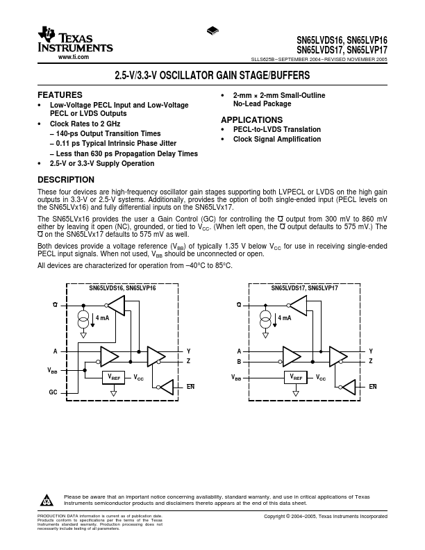
These four devices are high-frequency oscillator gain stages supporting both LVPECL or LVDS on the high gain outputs in 3.3-V or 2.5-V systems.
Key Features
- Low-Voltage PECL Input and Low-Voltage PECL or LVDS Outputs
- Clock Rates to 2 GHz – 140-ps Output Transition Times – 0.11 ps Typical Intrinsic Phase Jitter – Less than 630 ps Propagation Delay Times
- 2.5-V or 3.3-V Supply Operation
- 2-mm × 2-mm Small-Outline No-Lead Package
Applications
- PECL-to-LVDS Translation