SN74ABTH162260 Overview
Key Specifications
Package: SSOP
Mount Type: Surface Mount
Pins: 56
Operating Voltage: 5 V
Description
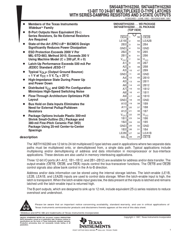
WD PACKAGE SN74ABTH162260. DL PACKAGE (TOP VIEW) OEA 1 LE1B 2 2B3 3 GND 4 2B2 5 2B1 6 VCC 7 A1 8 A2 9 A3 10 GND 11 A4 12 A5 13 A6 14 A7 15 A8 16 A9 17 GND 18 A10 19 A11 20 A12 21 VCC 22 1B1 23 1B2 24 GND 25 1B3 26 LE2B 27 SEL 28 56 OE2B 55 LEA2B 54 2B4 53 GND 52 2B5 51 2B6 50 VCC 49 2B7 48 2B8 47 2B9 46 GND 45 2B10 44 2B11 43 2B12 42 1B12 41 1B11 40 1B10 39 GND 38 1B9 37 1B8 36 1B7 35 VCC 34 1B6 33 1B5 32 GND 31 1B4 30 LEA1B 29 OE1B The ’ABTH162260 are 12-bit to 24-bit multiplexed D-type latches used in applications where two separate data paths must be multiplexed onto, or demultiplexed from, a single data path.