SN74ACT7813
SN74ACT7813 is 64 x 18 CLOCKED FIRST-IN FIRST-OUT MEMORY manufactured by Texas Instruments.
description
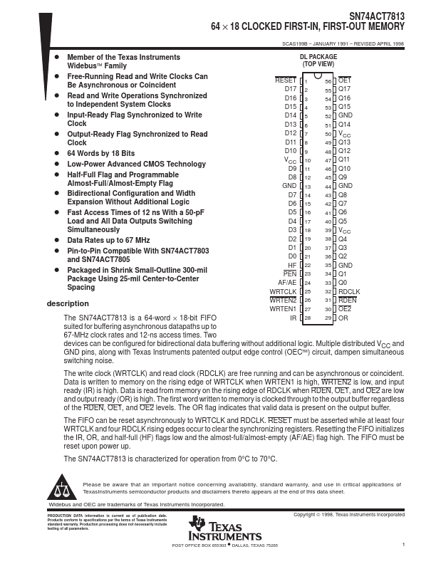
WRTEN2 26 WRTEN1 27
31 RDEN 30 OE2
The SN74ACT7813 is a 64-word × 18-bit FIFO
IR 28 29 OR suited for buffering asynchronous datapaths up to
67-MHz clock rates and 12-ns access times. Two devices can be configured for bidirectional data buffering without additional logic. Multiple distributed VCC and GND pins, along with Texas Instruments patented output edge control (OEC™) circuit, dampen simultaneous switching noise.
The write clock (WRTCLK) and read clock (RDCLK) are free running and can be asynchronous or coincident. Data is written to memory on the rising edge of WRTCLK when WRTEN1 is high, WRTEN2 is low, and input ready (IR) is high. Data is read from memory on the rising edge of RDCLK when RDEN, OE1, and OE2 are low and output ready (OR) is high. The first word written to memory is clocked through to the output buffer regardless of the RDEN, OE1, and OE2 levels. The OR flag indicates that valid data is present on the output buffer.
The FIFO can be reset asynchronously to WRTCLK and RDCLK. RESET must be asserted while at least four WRTCLK and four RDCLK rising edges occur to clear the synchronizing registers. Resetting the FIFO initializes the IR, OR, and half-full (HF) flags low and the almost-full/almost-empty (AF/AE) flag high. The FIFO must be reset upon power up.
The SN74ACT7813 is characterized for operation from 0°C to 70°C.
Please be aware that an important notice concerning availability, standard warranty, and use in critical applications of Texas Instruments semiconductor products and disclaimers thereto appears at the end of this data sheet.
Widebus and OEC are trademarks of Texas Instruments Incorporated.
PRODUCTION DATA information is current as of publication date. Products conform to specifications per the terms...