SN74AUC1G125
Features
- 1 Latch-Up Performance Exceeds 100 m A Per JESD 78, Class II
- ESD Protection Exceeds JESD 22
- 2000-V Human-Body Model (A114-A)
- 200-V Machine Model (A115-A)
- 1000-V Charged-Device Model (C101)
- Available in the Texas Instruments Nano Free™ Package
- Optimized for 1.8-V Operation and Is 3.6-V I/O Tolerant to Support Mixed-Mode Signal Operation
- Ioff Supports Partial Power Down Mode and Back Drive Protection
- Sub-1-V Operable
- Max tpd of 2.5 ns at 1.8 V
- Low Power Consumption, 10-µA Maximum ICC
- ±8-m A Output Drive at 1.8 V
3 Description
This bus buffer gate is operational at 0.8-V to 2.7-V VCC, but is designed specifically for 1.65-V to 1.95-V VCC operation.
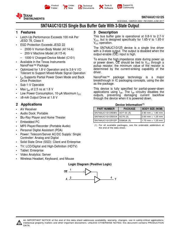
The SN74AUC1G125 device is a single line driver with a 3-state output. The output is disabled when the output-enable (OE) input is high.
To ensure the high-impedance state during power up or power down, OE should be tied to VCC through a pullup resistor; the minimum value of the resistor is determined by the...