SN74AUC1G126
Features
- 1 Latch-Up Performance Exceeds 100 m A Per JESD 78, Class II
- ESD Protection Exceeds JESD22
- 2000-V Human-Body Model (A114-A)
- 200-V Machine Model (A115-A)
- 1000-V Charged-Device Model (C101)
- Available in TI's Nano Free™ Package
- Optimized for 1.8-V Operation and is 3.6-V I/O
Tolerant to Support Mixed-Mode Signal Operation
- Ioff Supports Partial Power Down Mode and Back
Drive Protection
- Sub-1 V Operable
- Maximum tpd of 2.5 ns at 1.8 V
- Low Power Consumption, 10-µA Maximum ICC
- ±8-m A Output Drive at 1.8 V
2 Applications
- AV Receiver
- Audio Dock: Portable
- Blu-ray™ Player and Home Theater
- Embedded PC
- MP3 Player/Recorder (Portable Audio)
- Personal Digital Assistant (PDA)
- Power: AC/DC Supply, Single Controller
- Solid State Drive (SSD): Client and Enterprise
- TV: LCD, Digital, and High-Definition (HD)
- Tablet: Enterprise
- Video Analytics: Server
- Wireless Headset, Keyboard, and Mouse
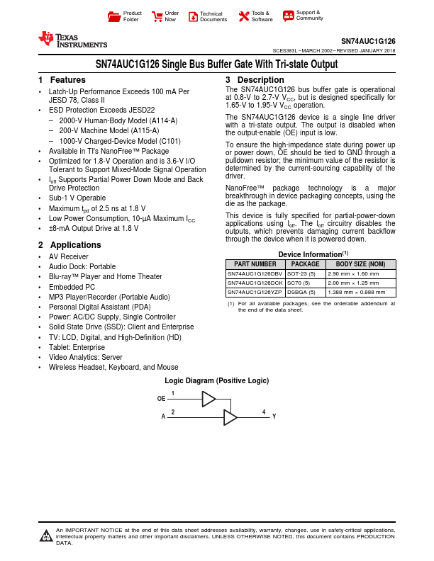
3 Description
The SN74AUC1G126 bus buffer gate is operational at 0.8-V...