Download SN74AUP1G34 Datasheet PDF
SN74AUP1G34 page 2
Page 2
SN74AUP1G34 page 3
Page 3

SN74AUP1G34 Description

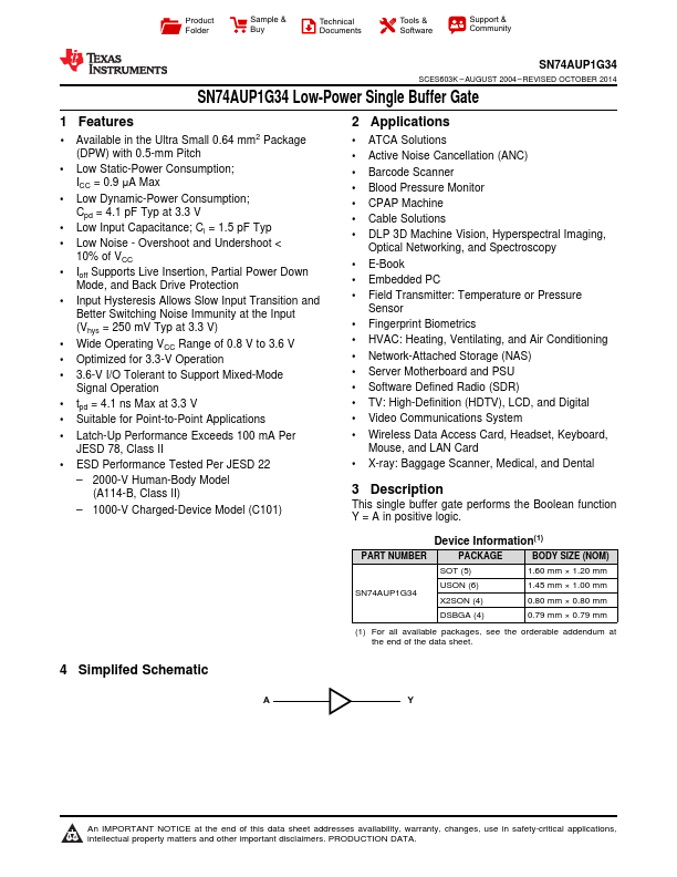
This single buffer gate performs the Boolean function Y = A in positive logic. 4 Simplifed Schematic A Y 1 An IMPORTANT NOTICE at the end of this data sheet addresses availability, warranty, changes, use in safety-critical applications, intellectual property matters and other important disclaimers. SN74AUP1G34 SCES603K AUGUST 2004 REVISED OCTOBER 2014 .ti.

SN74AUP1G34 Key Features

  • 1 Available in the Ultra Small 0.64 mm2 Package (DPW) with 0.5-mm Pitch
  • Low Static-Power Consumption; ICC = 0.9 μA Max
  • Low Dynamic-Power Consumption; Cpd = 4.1 pF Typ at 3.3 V
  • Low Input Capacitance; Ci = 1.5 pF Typ
  • Low Noise
  • Overshoot and Undershoot <
  • Ioff Supports Live Insertion, Partial Power Down
  • Input Hysteresis Allows Slow Input Transition and Better Switching Noise Immunity at the Input (Vhys = 250 mV Typ at 3.3
  • Wide Operating VCC Range of 0.8 V to 3.6 V
  • Optimized for 3.3-V Operation

SN74AUP1G34 Applications

  • Latch-Up Performance Exceeds 100 mA Per JESD 78, Class II
  • ESD Performance Tested Per JESD 22