SN74HCT125D
Overview
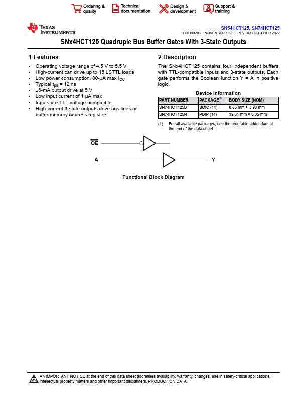
The SNx4HCT125 contains four independent buffers with TTL-compatible inputs and 3-state outputs. Each gate performs the Boolean function Y = A in positive logic.
- Operating voltage range of 4.5 V to 5.5 V
- High-current can drive up to 15 LSTTL loads
- Low power consumption, 80-µA max ICC
- Typical tpd = 12 ns
- ±6-mA output drive at 5 V
- Low input current of 1 µA max
- Inputs are TTL-voltage compatible
- High-current 3-state outputs drive bus lines or buffer memory address registers