SN74HCT139
Description
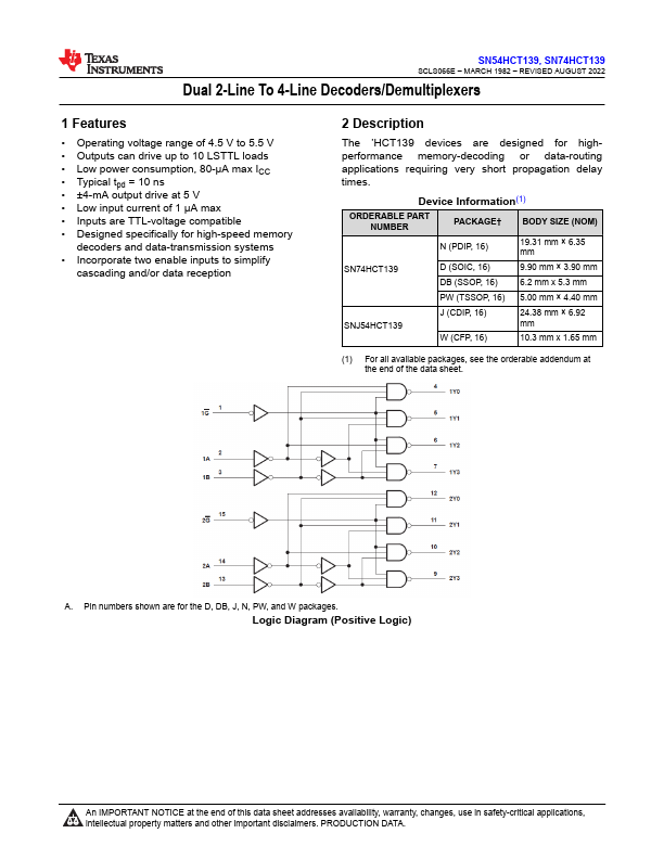
The ’HCT139 devices are designed for highperformance memory-decoding or data-routing applications requiring very short propagation delay times. Device Information(1) ORDERABLE PART NUMBER PACKAGE† BODY SIZE (NOM) N (PDIP, 16) 19.31 mm × 6.35 mm SN74HCT139 D (SOIC, 16) DB (SSOP, 16) 9.90 mm × 3.90 mm 6.2 mm x 5.3 mm PW (TSSOP, 16) 5.00 mm × 4.40 mm SNJ54HCT139 J (CDIP, 16) W (CFP, 16) 24.38 mm × 6.92 mm 10.3 mm x 1.65 mm (1) For all available packages, see the orderable addendum at the end of the data sheet.
Key Features
- Operating voltage range of 4.5 V to 5.5 V
- Outputs can drive up to 10 LSTTL loads
- Low power consumption, 80-µA max ICC
- Typical tpd = 10 ns
- ±4-mA output drive at 5 V
- Low input current of 1 µA max
- Inputs are TTL-voltage compatible
- Designed specifically for high-speed memory decoders and data-transmission systems
- Incorporate two enable inputs to simplify cascading and/or data reception