Overview
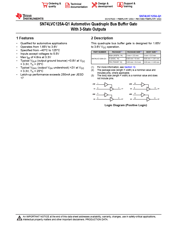
This quadruple bus buffer gate is designed for 1.65V to 3.6V VCC operation. PART NUMBER SN74LVC125A-Q1 PACKAGE(1) BQA (WQFN, 14) D (SOIC, 14) PW (TSSOP, 14) PACKAGE SIZE(2) BODY SIZE(3) 3 mm × 2.5 mm 3 mm × 2.5 mm 8.65 mm × 6 mm 8.65 mm × 3.91 mm 5.00 mm × 6.4 mm 5.00 mm × 4.40 mm (1) For more information, see Section 10. (2) The package size (length × width) is a nominal value and includes pins, where applicable. (3) The body size (length × width) is a nominal value and does not include pins. 1 1OE 2 1A 3 1Y 10 3OE 9 3A 8 3Y 4 2OE 5 2A 6 2Y 13 4OE 12 4A 11 4Y Logic Diagram (Positive Logic) An IMPORTANT NOTICE at the end of this data sheet addresses availability, warranty, changes, use in safety-critical applications, intellectual property matters and other important disclaimers.
- Qualified for automotive applications
- Operates from 1.65V to 3.6V
- Specified from -40°C to 125°C
- Inputs accept voltages to 5.5V
- Max tpd of 4.8ns at 3.3V
- Typical VOLP (output ground bounce) <0.8V at VCC = 3.3V, TA = 25°C
- Typical VOHV (output VOH undershoot) >2V at VCC = 3.3V, TA = 25°C
- Latch-up performance exceeds 250mA per JESD 17


