Datasheet4U Logo Datasheet4U.com

SN74LVC125A - Quadruple Bus Buffer Gate

General Description

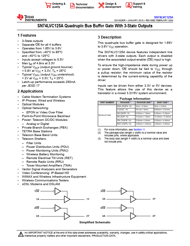
This quadruple bus buffer gate is designed for 1.65V to 3.6V VCC operation.

Key Features

  • 3-State outputs.
  • Separate OE for all 4 buffers.
  • Operates from 1.65V to 3.6V.
  • Specified from.
  • 40°C to 85°C and.
  • 40°C to 125°C.
  • Inputs accept voltages to 5.5V.
  • Max tpd of 4.8ns at 3.3V.
  • Typical VOLP (output ground bounce) < 0.8V at VCC = 3.3V, TA = 25°C.
  • Typical VOHV (output VOH undershoot) > 2V at VCC = 3.3V, TA = 25°C.
  • Latch-up performance exceeds 250mA per JESD 17 2.

📥 Download Datasheet

Full PDF Text Transcription for SN74LVC125A (Reference)

Note: Below is a high-fidelity text extraction (approx. 800 characters) for SN74LVC125A. For precise diagrams, and layout, please refer to the original PDF.

SN74LVC125A SCAS290R – JANUARY 2015 – REVISED FEBRUARY 2024 SN74LVC125A Quadruple Bus Buffer Gate With 3-State Outputs 1 Features • 3-State outputs • Separate OE for all ...

View more extracted text
th 3-State Outputs 1 Features • 3-State outputs • Separate OE for all 4 buffers • Operates from 1.65V to 3.6V • Specified from –40°C to 85°C and –40°C to 125°C • Inputs accept voltages to 5.5V • Max tpd of 4.8ns at 3.3V • Typical VOLP (output ground bounce) < 0.8V at VCC = 3.3V, TA = 25°C • Typical VOHV (output VOH undershoot) > 2V at VCC = 3.