Datasheet4U Logo Datasheet4U.com

SN74LVC1G00 - Single 2-Input Positive-NAND Gate

General Description

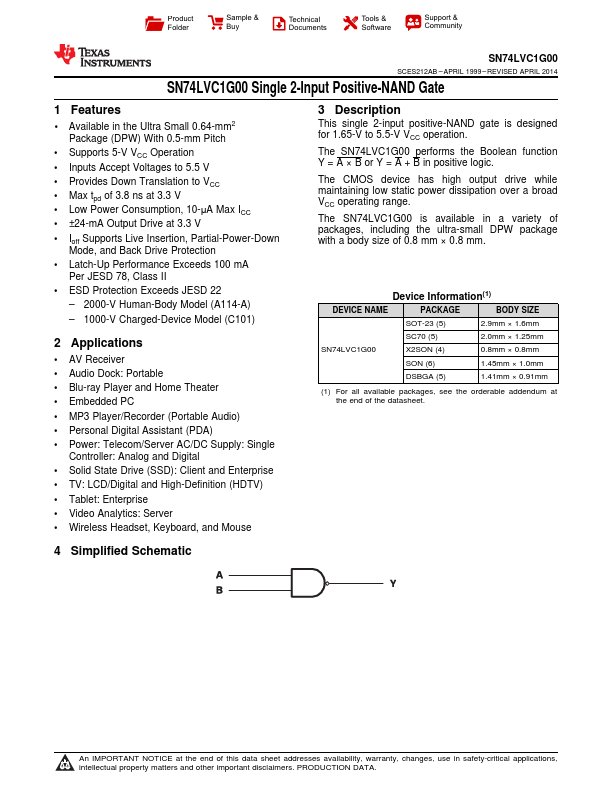
This single 2-input positive-NAND gate is designed for 1.65-V to 5.5-V VCC operation.

The SN74LVC1G00 performs the Boolean function Y = A × B or Y = A + B in positive logic.

The CMOS device has high output drive while maintaining low static power dissipation over a broad VCC operating range.

Key Features

  • 1 Available in the Ultra Small 0.64-mm2 Package (DPW) With 0.5-mm Pitch.
  • Supports 5-V VCC Operation.
  • Inputs Accept Voltages to 5.5 V.
  • Provides Down Translation to VCC.
  • Max tpd of 3.8 ns at 3.3 V.
  • Low Power Consumption, 10-μA Max ICC.
  • ±24-mA Output Drive at 3.3 V.
  • Ioff Supports Live Insertion, Partial-Power-Down Mode, and Back Drive Protection.
  • Latch-Up Performance Exceeds 100 mA Per JESD 78, Class II.
  • ESD P.

📥 Download Datasheet

Full PDF Text Transcription (Reference)

The following content is an automatically extracted verbatim text from the original manufacturer datasheet and is provided for reference purposes only.

View original datasheet text
Product Folder Sample & Buy Technical Documents Tools & Software Support & Community SN74LVC1G00 SCES212AB – APRIL 1999 – REVISED APRIL 2014 SN74LVC1G00 Single 2-Input Positive-NAND Gate 1 Features •1 Available in the Ultra Small 0.64-mm2 Package (DPW) With 0.5-mm Pitch • Supports 5-V VCC Operation • Inputs Accept Voltages to 5.5 V • Provides Down Translation to VCC • Max tpd of 3.8 ns at 3.3 V • Low Power Consumption, 10-μA Max ICC • ±24-mA Output Drive at 3.