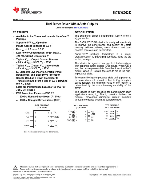
SN74LVC2G240
SN74LVC2G240 is Dual Buffer Driver manufactured by Texas Instruments.
.ti.
SCES208I
- APRIL 1999
- REVISED NOVEMBER 2013
Dual Buffer Driver With 3-State Outputs
Check for Samples: SN74LVC2G240
Features
- 2 Available in the Texas Instruments NanoFree™ Package
- Supports 5-V VCC Operation
- Inputs Accept Voltages to 5.5 V
- Max tpd of 4.6 ns at 3.3 V
- Low Power Consumption, 10-µA Max ICC
- ±24-mA Output Drive at 3.3 V
- Typical VOLP (Output Ground Bounce) <0.8 V at VCC = 3.3 V, TA = 25°C
- Typical VOHV (Output VOH Undershoot) >2 V at VCC = 3.3 V, TA = 25°C
- Ioff Supports Live Insertion, Partial-PowerDown Mode, and Back-Drive Protection
- Can Be Used as a Down Translator to Translate Inputs From a Max of 5.5 V Down to the VCC Level
-...