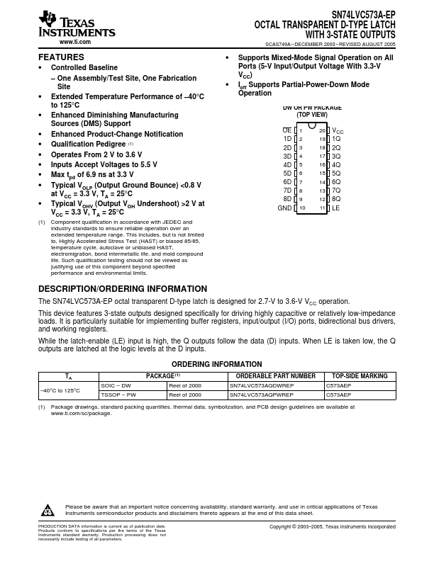
• Part: SN74LVC573A-EP
  • Description: OCTAL TRANSPARENT D-TYPE LATCH
  • Manufacturer: Texas Instruments
  • Size: 217.94 KB
Download SN74LVC573A-EP Datasheet PDF
Texas Instruments
SN74LVC573A-EP
SN74LVC573A-EP is OCTAL TRANSPARENT D-TYPE LATCH manufactured by Texas Instruments.
FEATURES - Controlled Baseline - One Assembly/Test Site, One Fabrication Site - Extended Temperature Performance of - 40°C to 125°C - Enhanced Diminishing Manufacturing Sources (DMS) Support - Enhanced Product-Change Notification - Qualification Pedigree (1) - Operates From 2 V to 3.6 V - Inputs Accept Voltages to 5.5 V - Max tpd of 6.9 ns at 3.3 V - Typical VOLP (Output Ground Bounce) <0.8 V at VCC = 3.3 V, TA = 25°C - Typical VOHV (Output VOH Undershoot) >2 V at VCC = 3.3 V, TA = 25°C (1) ponent qualification in accordance with JEDEC and industry standards to ensure reliable operation over an extended temperature range. This includes, but is not limited to, Highly Accelerated Stress Test (HAST) or biased 85/85, temperature cycle, autoclave or unbiased HAST, electromigration, bond intermetallic life, and mold pound life. Such qualification testing should not be viewed as justifying use of this ponent beyond specified performance and environmental limits. SN74LVC573A-EP OCTAL TRANSPARENT D-TYPE LATCH WITH 3-STATE OUTPUTS SCAS749A - DECEMBER 2003 - REVISED AUGUST 2005 - Supports Mixed-Mode Signal Operation on All Ports (5-V Input/Output Voltage With 3.3-V VCC) - Ioff Supports Partial-Power-Down Mode Operation DW OR PW PACKAGE (TOP VIEW) OE 1 1D 2 2D 3 3D 4 4D 5 5D 6 6D 7 7D 8 8D 9 GND 10 20 VCC 19 1Q 18 2Q 17 3Q 16 4Q 15 5Q 14 6Q 13 7Q 12 8Q 11 LE DESCRIPTION /ORDERING INFORMATION The SN74LVC573A-EP octal transparent D-type latch is designed for 2.7-V to 3.6-V VCC operation. This device features 3-state outputs designed specifically for driving highly capacitive or relatively low-impedance loads. It is particularly suitable for implementing buffer registers, input/output (I/O) ports, bidirectional bus drivers, and working registers. While the latch-enable (LE) input is high, the Q outputs follow the data (D) inputs. When LE is taken low, the Q outputs are latched at the logic levels at the D inputs. - 40°C to 125°C SOIC - DW TSSOP - PW ORDERING...