SN74SSTV32852
description
/ordering information
This 24-bit to 48-bit registered buffer is designed for 2.3-V to 2.7-V VCC operation.
All inputs are SSTL_2, except the LVCMOS reset (RESET) input. All outputs are SSTL_2, Class II patible.
The SN74SSTV32852 operates from a differential clock (CLK and CLK). Data are registered at the crossing of CLK going high and CLK going low.
The device supports low-power standby operation. When RESET is low, the differential input receivers are disabled, and undriven (floating) data, clock, and reference voltage (VREF) inputs are allowed. In addition, when RESET is low, all registers are reset and all outputs are forced low. The LVCMOS RESET input always must be held at a valid logic high or low level.
To ensure defined outputs from the register before a stable clock has been supplied, RESET must be held in the low state during power up.
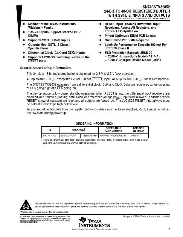
ORDERING INFORMATION
PACKAGE†
ORDERABLE PART NUMBER
TOP-SIDE MARKING
0°C to 70°C LFBGA
- GKF Tape and reel...