Datasheet Summary
Product Folder
Order Now
Technical Documents
Tools & Software
Support & munity
SLVSDF2A
- MAY 2017
- REVISED JULY 2017
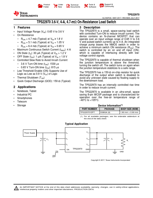
TPS22970 3.6-V, 4-A, 4.7-mΩ On-Resistance Load Switch
1 Features
- 1 Input Voltage Range (VIN): 0.65 V to 3.6 V
- On-Resistance
- RON = 4.7 mΩ (Typical) at VIN ≥ 1.8 V
- RON = 5.1 mΩ (Typical) at VIN = 1.05 V
- RON = 6.4 mΩ (Typical) at VIN = 0.65 V
- Maximum Continuous Switch Current (IMAX): 4 A
- ON State (IQ): 30 µA (Typical) at VIN > 1.2 V
- OFF State (ISD): 1 µA (Typical) at VIN > 1.8 V
- Controlled Slew Rate to Avoid Inrush Current
- 3.6 V Turn-ON time (tON): 1530 μs
- 0.65 V Turn-ON time (tON): 815 μs
- Low Threshold Enable (ON) Supports Use of...