TPS61253
TPS61253 is 3.5-MHz High Efficiency Step-Up Converter manufactured by Texas Instruments.
Product Folder
Sample & Buy
Technical Documents
Tools & Software
Support & munity
TPS61253, TPS61254, TPS61256, TPS61258, TPS61259, TPS612592
SLVSAG8G
- SEPTEMBER 2011
- REVISED JUNE 2016
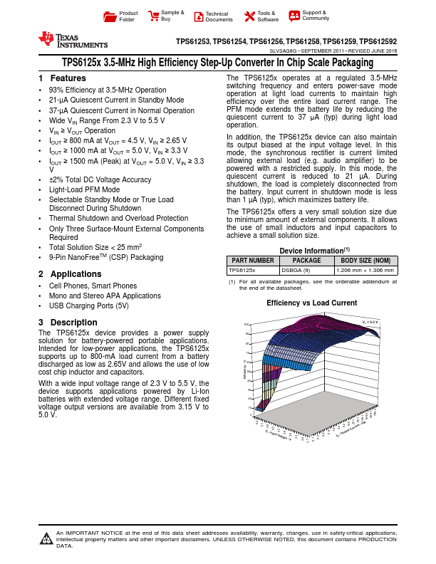
TPS6125x 3.5-MHz High Efficiency Step-Up Converter In Chip Scale Packaging
1 Features
- 1 93% Efficiency at 3.5-MHz Operation
- 21-µA Quiescent Current in Standby Mode
- 37-µA Quiescent Current in Normal Operation
- Wide VIN Range From 2.3 V to 5.5 V
- VIN ≥ VOUT Operation
- IOUT ≥ 800 m A at VOUT = 4.5 V, VIN ≥ 2.65 V
- IOUT ≥ 1000 m A at VOUT = 5.0 V, VIN ≥ 3.3 V
- IOUT ≥ 1500 m A (Peak) at VOUT = 5.0 V, VIN ≥ 3.3
- ±2% Total DC Voltage Accuracy
- Light-Load PFM Mode
- Selectable Standby Mode or True Load
Disconnect During Shutdown
- Thermal Shutdown and Overload Protection
- Only Three Surface-Mount External ponents
Required
- Total Solution Size < 25 mm2
- 9-Pin Nano Free TM (CSP) Packaging
2 Applications
- Cell Phones, Smart...