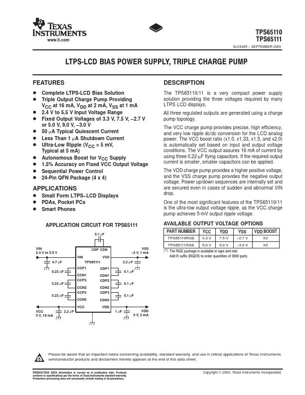
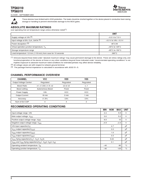
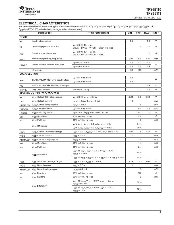
Datasheet4U Logo Datasheet4U.com

TPS65111 - LTPS-LCD BIAS POWER SUPPLY / TRIPLE CHARGE PUMP

This page provides the datasheet information for the TPS65111, a member of the TPS65110 LTPS-LCD BIAS POWER SUPPLY / TRIPLE CHARGE PUMP family.

Datasheet Summary

Description

The TPS65110/11 is a very compact power supply solution providing the three voltages required by many LTPS LCD displays.

All three regulated outputs are generated using a charge pump topology.

Features

  • D Complete LTPS-LCD Bias Solution D Triple Output Charge Pump Providing VCC at 16 mA, VDD at 2 mA, VSS at 1 mA D 2.4 V to 5.5 V Input Voltage Range D Fixed Output Voltages of 3.3 V, 7.5 V,.
  • 2.7 V or 5.0 V, 9.0 V,.
  • 3.0 V D 50 µA Typical Quiescent Current D Less Than 1 µA Shutdown Current D Ultra-Low Ripple (VCC = 5 mV, Typical at 5 mA) D Autonomous Boost for VCC Supply D 1.5% Accuracy on Fixed VCC Output Voltage D Sequential Power Control D 24-Pin QFN Package (4 x 4).

📥 Download Datasheet

Datasheet preview – TPS65111

Datasheet Details

Part number TPS65111
Manufacturer Texas Instruments
File Size 213.04 KB
Description LTPS-LCD BIAS POWER SUPPLY / TRIPLE CHARGE PUMP
Datasheet download datasheet TPS65111 Datasheet
Additional preview pages of the TPS65111 datasheet.
Other Datasheets by Texas Instruments

Full PDF Text Transcription

Click to expand full text
www.ti.com TPS65110 TPS65111 SLVS495 − SEPTEMBER 2003 LTPSĆLCD BIAS POWER SUPPLY, TRIPLE CHARGE PUMP FEATURES D Complete LTPS-LCD Bias Solution D Triple Output Charge Pump Providing VCC at 16 mA, VDD at 2 mA, VSS at 1 mA D 2.4 V to 5.5 V Input Voltage Range D Fixed Output Voltages of 3.3 V, 7.5 V, −2.7 V or 5.0 V, 9.0 V, −3.0 V D 50 µA Typical Quiescent Current D Less Than 1 µA Shutdown Current D Ultra-Low Ripple (VCC = 5 mV, Typical at 5 mA) D Autonomous Boost for VCC Supply D 1.5% Accuracy on Fixed VCC Output Voltage D Sequential Power Control D 24-Pin QFN Package (4 x 4) APPLICATIONS D Small Form LTPS−LCD Displays D PDAs, Pocket PCs D Smart Phones APPLICATION CIRCUIT FOR TPS65111 0.1 µF VIN 2.4 V to 5.5 V 4.7 µF 0.22 µF 0.22 µF 0.
Published: |