TPS9103
TPS9103 is POWER SUPPLY manufactured by Texas Instruments.
description
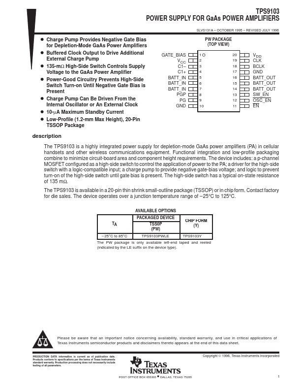
The TPS9103 is a highly integrated power supply for depletion-mode Ga As power amplifiers (PA) in cellular handsets and other wireless munications equipment. Functional integration and low-profile packaging bine to minimize circuit-board area and ponent height requirements. The device includes: a p-channel MOSFET configured as a high-side switch to control the application of power to the PA; a driver for the high-side switch with a logic-patible input; a charge pump to provide negative gate-bias voltage; and logic to prevent turn-on of the high-side switch until gate bias is present. The high-side switch has a typical on-state resistance of 135 mΩ.
The TPS9103 is available in a 20-pin thin shrink small-outline package (TSSOP) or in chip form. Contact factory for die sales. The device operates over a junction temperature range of
- 25°C to 125°C.
AVAILABLE OPTIONS
PACKAGED DEVICE
CHIP FORM
TSS0P
(Y)
(PW)
- 25°C to 85°C
TPS9103PWLE
TPS9103Y
The PW package is only available left-end taped and reeled (indicated by the LE suffix on the device type).
Please be aware that an important notice concerning availability, standard warranty, and use in critical applications of Texas Instruments semiconductor products and disclaimers thereto appears at the end of this data sheet.
PRODUCTION DATA information is current as of publication date. Products conform to specifications per the terms of Texas Instruments standard warranty. Production processing does not necessarily include testing of all parameters.
- POST OFFICE BOX 655303 DALLAS, TEXAS 75265
Copyright © 1996, Texas Instruments Incorporated 1
TPS9103 POWER SUPPLY FOR Ga As POWER AMPLIFIERS
SLVS131A
- OCTOBER 1995
- REVISED JULY 1996 functional block diagram
BATT_IN 5, 6, 7 VCC 2
3 VCC
UVLO
18 BCLK
VDD 20
EN 11 OSC_EN 12
REF +
Vref
PGP 8
C1 + 4 C1
- 3
Inverting Charge Pump
GND 10,...