TPS9110
TPS9110 is CELLULAR SUBSCRIBER TERMINAL POWER SUPPLY manufactured by Texas Instruments.
description
CELLULAR SUBSCRIBER TERMINAL
POWER SUPPLY
SLVS164
- AUGUST 1997
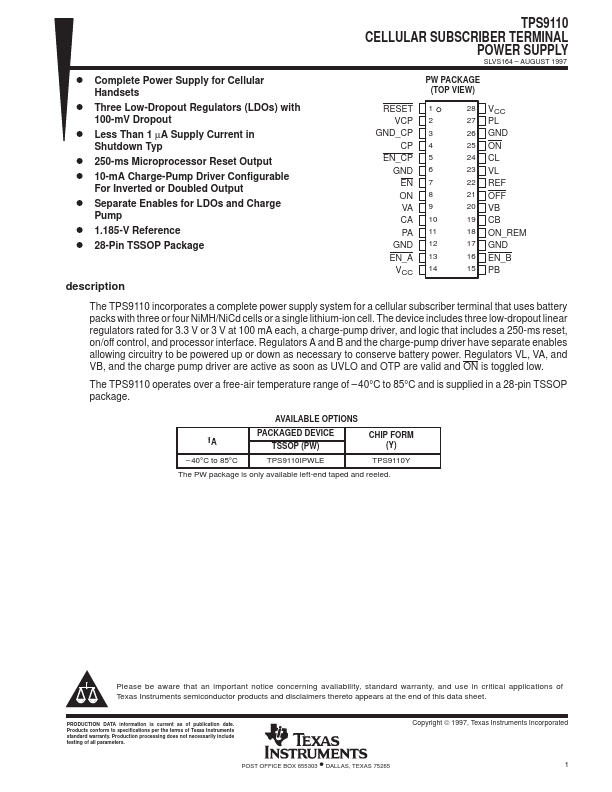
PW PACKAGE (TOP VIEW)
RESET VCP
GND_CP CP
EN_CP GND EN ON VA CA PA GND EN_A VCC
1 2 3 4 5 6 7 8 9 10 11 12 13 14
28 VCC 27 PL
26 GND 25 ON 24 CL 23 VL 22 REF 21 OFF 20 VB 19 CB 18 ON_REM 17 GND 16 EN_B 15 PB
The TPS9110 incorporates a plete power supply system for a cellular subscriber terminal that uses battery packs with three or four Ni MH/Ni Cd cells or a single lithium-ion cell. The device includes three low-dropout linear regulators rated for 3.3 V or 3 V at 100 m A each, a charge-pump driver, and logic that includes a 250-ms reset, on/off control, and processor interface. Regulators A and B and the charge-pump driver have separate enables allowing circuitry to be powered up or down as necessary to conserve battery power. Regulators VL, VA, and VB, and the charge pump driver are active as soon as UVLO and OTP are valid and ON is toggled low.
The TPS9110 operates over a free-air temperature range of
- 40°C to 85°C and is supplied in a 28-pin TSSOP package.
AVAILABLE OPTIONS
PACKAGED DEVICE TSSOP (PW)
CHIP FORM (Y)
- 40°C to 85°C
TPS9110IPWLE
TPS9110Y
The PW package is only available left-end taped and reeled.
Please be aware that an important notice concerning availability, standard warranty, and use in critical applications of Texas Instruments semiconductor products and disclaimers thereto appears at the end of this data sheet.
PRODUCTION DATA information is current as of publication date. Products conform to specifications per the terms of Texas Instruments standard warranty. Production processing does not necessarily include testing of all parameters.
- POST OFFICE BOX 655303 DALLAS, TEXAS 75265
Copyright © 1997, Texas Instruments Incorporated 1
TPS9110 CELLULAR SUBSCRIBER TERMINAL POWER SUPPLY
SLVS164
- AUGUST 1997 functional block diagram
EN REF
EN_A
EN_B GND
Voltage Reference
UVLO† and OTP‡
ON_REM
†...