UCC27211A Overview
Description
The UCC27211A device driver is based on the popular UCC27201 MOSFET drivers; but, this device offers several significant performance improvements. The peak output pullup and pulldown current has been increased to 3.7A source and 4.5A sink and +12V +100V VDD HB SECONDARY SIDE CIRCUIT HI PWM CONTROLLER LI DRIVE HO HI HS DRIVE LO LO UCC27211A VSS ISOLATION AND FEEDBACK.
Key Features
- 40°C to +150°C junction temperature range
- Drives two N-channel MOSFETs in high-side and low-side configuration with independent inputs
- Maximum boot voltage 120V DC
- 3.7A source, 4.5A sink output currents
- Input pins can tolerate –10V to +20V and are independent of supply voltage range
- TTL compatible inputs
- 8V to 17V VDD operating range, (20V ABS MAX)
- 7.2ns rise and 5.5ns fall time with 1000pF load
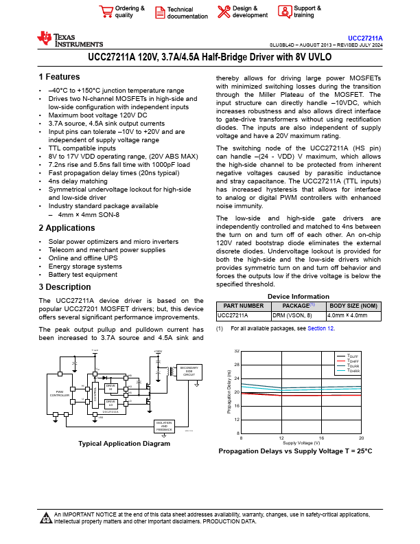
- Fast propagation delay times (20ns typical)
- 4ns delay matching