74AHCT74
74AHCT74 is Dual D-type flip-flop manufactured by Nexperia.
- Part of the 74AHC74 comparator family.
- Part of the 74AHC74 comparator family.
description
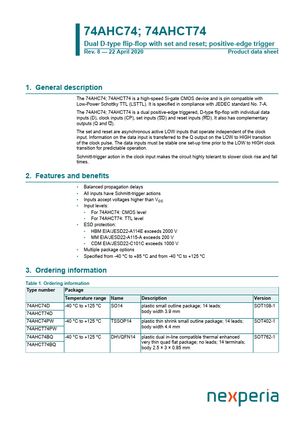
The 74AHC74; 74AHCT74 is a high-speed Si-gate CMOS device and is pin patible with Low-Power Schottky TTL (LSTTL). It is specified in pliance with JEDEC standard No. 7-A.
The 74AHC74; 74AHCT74 is a dual positive-edge triggered, D-type flip-flop with individual data inputs (D), clock inputs (CP), set inputs (SD) and reset inputs (RD). It also has plementary outputs (Q and Q).
The set and reset are asynchronous active LOW inputs that operate independent of the clock input. Information on the data input is transferred to the Q output on the LOW to HIGH transition of the clock pulse. The data inputs must be stable one set-up time prior to the LOW to HIGH clock transition for predictable operation.
Schmitt-trigger action in the clock input makes the circuit highly tolerant to slower clock rise and fall times.
2. Features and benefits
- Balanced propagation delays
- All inputs have Schmitt-trigger actions
- Inputs accept voltages higher than VCC
- Input levels:
- For 74AHC74: CMOS level
- For 74AHCT74: TTL level
- ESD protection:
- HBM EIA/JESD22-A114E exceeds 2000 V
- MM EIA/JESD22-A115-A exceeds 200 V
- CDM EIA/JESD22-C101C exceeds 1000 V
- Multiple package options
- Specified from -40 °C to +85 °C and from -40 °C to +125 °C
3. Ordering information
Table 1. Ordering information Type number Package
Temperature range Name
74AHC74D
-40 °C to +125 °C SO14
74AHCT74D
74AHC74PW -40 °C to +125 °C TSSOP14
74AHCT74PW
74AHC74BQ
-40 °C to +125 °C DHVQFN14
74AHCT74BQ
Description plastic small outline package; 14 leads; body width 3.9 mm plastic thin shrink small outline package; 14 leads; body width 4.4 mm plastic dual in-line patible thermal enhanced very thin quad flat package; no leads; 14 terminals; body 2.5 × 3 × 0.85 mm
Version SOT108-1
SOT402-1
SOT762-1
Nexperia
74AHC74; 74AHCT74
Dual D-type flip-flop with set and reset; positive-edge trigger
4. Functional diagram
4 10 1SD 2SD
2...


