Nexperia 74ALVCH16821
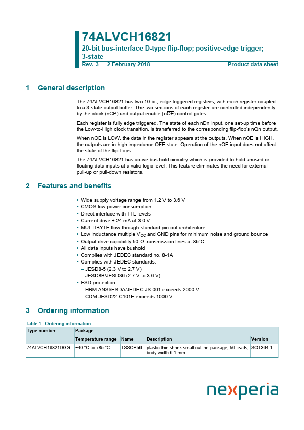
The 74ALVCH16821 has two 10-bit, edge triggered registers, with each register coupled to a 3-state output buffer. The two sections of each register are controlled independently by the clock (nCP) and output enable (nOE) control gates. Each register is fully edge triggered.| Part No. | 74ALVCH16821 |
|---|---|
| Datasheet | 74ALVCH16821 Download |
| Manufacturer |  Nexperia |
| Description | 20-bit bus-interface D-type flip-flop |
| Buy | Stock & Price |
FEATURES AND BENEFITS
● Wide supply voltage range from 1.2 V to 3.6 V● CMOS low-power consumption
● Direct interface with TTL levels
● Current drive ± 24 mA at 3.0 V
● MULTIBYTE flow-through standard pin-out architecture
● Low inductance multiple VCC and GND pins for minimum noise and ground bounce
● Output drive capability 50 Ω transmission lines at 85°C
● All data inputs have bushold
● Complies with JEDEC standard no. 8-1A
● Complies with JEDEC standards: – JESD8-5 (2.3 V to 2.7 V) – JESD8B/JESD36 (2.7 V to 3.6 V)
● ESD protection: – HBM ANSI/ESDA/JEDEC JS-001 exceeds 2000 V – CDM JESD22-C101E exceeds 1000 V 3 Ordering information Table 1. Ordering information Type number Package Temperature range Name
DESCRIPTION
Version 74ALVCH16821DGG −40 °C to +85 °C TSSOP56 plastic thin shrink small outline package; 56 leads; SOT364-1 body width 6.1 mm Nexperia 74ALVCH16821 20-bit bus-interface D-type flip-flop; positive-edge trigger; 3-state 4 Functional diagram 55 54 52 51 49 48 47 45 44 43 1...
