Datasheet4U Logo Datasheet4U.com

74AUP1G07-Q100 - Low-power buffer

General Description

The 74AUP1G07-Q100 is a single buffer with open-drain output.

Schmitt-trigger action at all inputs makes the circuit tolerant of slower input rise and fall times.

This device ensures a very low static and dynamic power consumption across the entire VCC range from 0.8 V to 3.6 V.

Key Features

  • Automotive product qualification in accordance with AEC-Q100 (Grade 1).
  • Specified from -40 °C to +85 °C and from -40 °C to +125 °C.
  • Wide supply voltage range from 0.8 V to 3.6 V.
  • High noise immunity.
  • CMOS low power dissipation.
  • Complies with JEDEC standards:.
  • JESD8-12 (0.8 V to 1.3 V).
  • JESD8-11 (0.9 V to 1.65 V).
  • JESD8-7 (1.65 V to 1.95 V).
  • JESD8-5 (2.3 V to 2.7 V).
  • JESD8C (2.7 V to 3.6 V).

📥 Download Datasheet

Full PDF Text Transcription (Reference)

The following content is an automatically extracted verbatim text from the original manufacturer datasheet and is provided for reference purposes only.

View original datasheet text
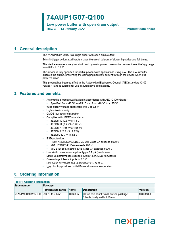
74AUP1G07-Q100 Low-power buffer with open-drain output Rev. 3 — 13 January 2022 Product data sheet 1. General description The 74AUP1G07-Q100 is a single buffer with open-drain output. Schmitt-trigger action at all inputs makes the circuit tolerant of slower input rise and fall times. This device ensures a very low static and dynamic power consumption across the entire VCC range from 0.8 V to 3.6 V. This device is fully specified for partial power-down applications using IOFF. The IOFF circuitry disables the output, preventing the damaging backflow current through the device when it is powered down. This product has been qualified to the Automotive Electronics Council (AEC) standard Q100 (Grade 1) and is suitable for use in automotive applications. 2.