Datasheet4U Logo Datasheet4U.com

74AUP1G97 - Low-power configurable multiple function gate

Description

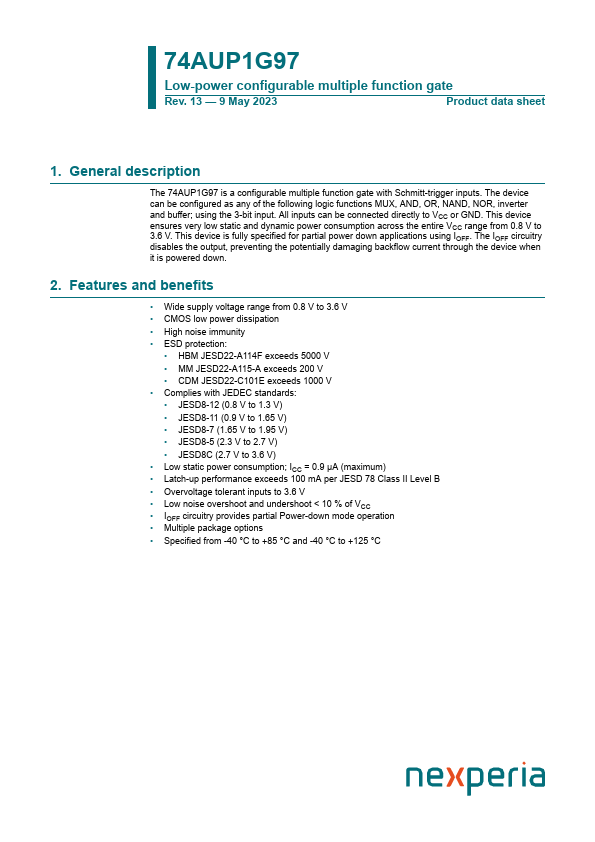
The 74AUP1G97 is a configurable multiple function gate with Schmitt-trigger inputs.

The device can be configured as any of the following logic functions MUX, AND, OR, NAND, NOR, inverter and buffer; using the 3-bit input.

All inputs can be connected directly to VCC or GND.

Features

  • Wide supply voltage range from 0.8 V to 3.6 V.
  • CMOS low power dissipation.
  • High noise immunity.
  • ESD protection:.
  • HBM JESD22-A114F exceeds 5000 V.
  • MM JESD22-A115-A exceeds 200 V.
  • CDM JESD22-C101E exceeds 1000 V.
  • Complies with JEDEC standards:.
  • JESD8-12 (0.8 V to 1.3 V).
  • JESD8-11 (0.9 V to 1.65 V).
  • JESD8-7 (1.65 V to 1.95 V).
  • JESD8-5 (2.3 V to 2.7 V).
  • JESD8C (2.7 V to 3.6 V).

📥 Download Datasheet

Datasheet preview – 74AUP1G97

Datasheet Details

Part number 74AUP1G97
Manufacturer nexperia
File Size 295.67 KB
Description Low-power configurable multiple function gate
Datasheet download datasheet 74AUP1G97 Datasheet
Additional preview pages of the 74AUP1G97 datasheet.
Other Datasheets by nexperia

Full PDF Text Transcription

Click to expand full text
74AUP1G97 Low-power configurable multiple function gate Rev. 13 — 9 May 2023 Product data sheet 1. General description The 74AUP1G97 is a configurable multiple function gate with Schmitt-trigger inputs. The device can be configured as any of the following logic functions MUX, AND, OR, NAND, NOR, inverter and buffer; using the 3-bit input. All inputs can be connected directly to VCC or GND. This device ensures very low static and dynamic power consumption across the entire VCC range from 0.8 V to 3.6 V. This device is fully specified for partial power down applications using IOFF. The IOFF circuitry disables the output, preventing the potentially damaging backflow current through the device when it is powered down. 2. Features and benefits • Wide supply voltage range from 0.8 V to 3.
Published: |