Datasheet4U Logo Datasheet4U.com

74AUP1T34-Q100 - Low-power dual supply translating buffer

General Description

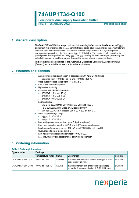
The 74AUP1T34-Q100 is a single dual supply translating buffer.

Input A is referenced to VCC(A) and output Y is referenced to VCC(Y).

Schmitt-trigger action at all inputs makes the circuit tolerant of slower input rise and fall times.

Key Features

  • Automotive product qualification in accordance with AEC-Q100 (Grade 1).
  • Specified from -40 °C to +85 °C and -40 °C to +125 °C.
  • Wide supply voltage range from 1.1 V to 3.6 V.
  • CMOS low power dissipation.
  • High noise immunity.
  • Complies with JEDEC standards:.
  • JESD8-7 (1.2 V to 1.95 V).
  • JESD8-5 (1.8 V to 2.7 V).
  • JESD8-B (2.7 V to 3.6 V).
  • ESD protection:.
  • MIL-STD-883, method 3015 Class 3A. Exceeds 5000 V.

📥 Download Datasheet

Datasheet Details

Part number 74AUP1T34-Q100
Manufacturer Nexperia
File Size 275.13 KB
Description Low-power dual supply translating buffer
Datasheet download datasheet 74AUP1T34-Q100 Datasheet

Full PDF Text Transcription (Reference)

The following content is an automatically extracted verbatim text from the original manufacturer datasheet and is provided for reference purposes only.

View original datasheet text
74AUP1T34-Q100 Low-power dual supply translating buffer Rev. 4 — 25 January 2022 Product data sheet 1. General description The 74AUP1T34-Q100 is a single dual supply translating buffer. Input A is referenced to VCC(A) and output Y is referenced to VCC(Y). Schmitt-trigger action at all inputs makes the circuit tolerant of slower input rise and fall times. This device ensures very low static and dynamic power consumption across the entire VCC range from 1.1 V to 3.6 V. This device is fully specified for partial power down applications using IOFF. The IOFF circuitry disables the output, preventing the potentially damaging backflow current through the device when it is powered down.