Datasheet4U Logo Datasheet4U.com
Nexperia logo

74AUP2G80 Datasheet

Manufacturer: Nexperia
74AUP2G80 datasheet preview

Datasheet Details

Part number 74AUP2G80
Datasheet 74AUP2G80-nexperia.pdf
File Size 274.87 KB
Manufacturer Nexperia
Description Low-power dual D-type flip-flop
74AUP2G80 page 2 74AUP2G80 page 3

74AUP2G80 Overview

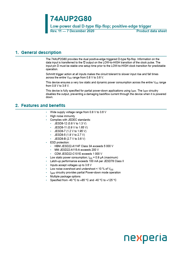
The 74AUP2G80 provides the dual positive-edge triggered D-type flip-flop. Information on the data input is transferred to the Q output on the LOW-to-HIGH transition of the clock pulse. The input pin D must be stable one setup time prior to the LOW-to-HIGH clock transition for predictable operation.

74AUP2G80 Key Features

  • Wide supply voltage range from 0.8 V to 3.6 V
  • High noise immunity
  • plies with JEDEC standards
  • JESD8-12 (0.8 V to 1.3 V)
  • JESD8-11 (0.9 V to 1.65 V)
  • JESD8-7 (1.2 V to 1.95 V)
  • JESD8-5 (1.8 V to 2.7 V)
  • JESD8-B (2.7 V to 3.6 V)
  • ESD protection
  • HBM JESD22-A114F Class 3A exceeds 5 000 V

74AUP2G80 Applications

  • Wide supply voltage range from 0.8 V to 3.6 V

74AUP2G80 from other manufacturers

See all manufacturers

Brand Logo Part Number Description Other Manufacturers
NXP Logo 74AUP2G80 Low-power dual D-type flip-flop NXP
Nexperia logo - Manufacturer

More Datasheets from Nexperia

See all Nexperia datasheets

Part Number Description
74AUP2G86 Low-power dual 2-input EXCLUSIVE-OR gate
74AUP2G00 Low-power dual 2-input NAND gate
74AUP2G00-Q100 Low-power dual 2-input NAND gate
74AUP2G02 Low-power dual 2-input NOR gate
74AUP2G04 Low-power dual inverter
74AUP2G04-Q100 Low-power dual inverter
74AUP2G06 Low-power dual inverter
74AUP2G0604 Low-power inverting buffer
74AUP2G07 Low-power dual buffer
74AUP2G08 Low-power dual 2-input AND gate

74AUP2G80 Distributor

Datasheet4U Logo
Since 2006. D4U Semicon. About Datasheet4U Contact Us Privacy Policy Purchase of parts