Datasheet4U Logo Datasheet4U.com

74LVC1G10 - Single 3-input NAND gate

Description

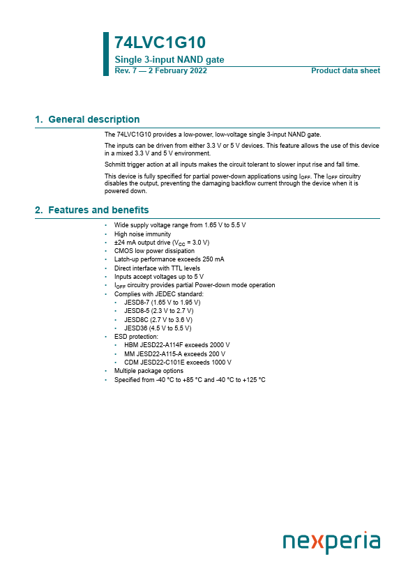
The 74LVC1G10 provides a low-power, low-voltage single 3-input NAND gate.

The inputs can be driven from either 3.3 V or 5 V devices.

This feature allows the use of this device in a mixed 3.3 V and 5 V environment.

Features

  • Wide supply voltage range from 1.65 V to 5.5 V.
  • High noise immunity.
  • ±24 mA output drive (VCC = 3.0 V).
  • CMOS low power dissipation.
  • Latch-up performance exceeds 250 mA.
  • Direct interface with TTL levels.
  • Inputs accept voltages up to 5 V.
  • IOFF circuitry provides partial Power-down mode operation.
  • Complies with JEDEC standard:.
  • JESD8-7 (1.65 V to 1.95 V).
  • JESD8-5 (2.3 V to 2.7 V).
  • JESD8C (2.

📥 Download Datasheet

Datasheet preview – 74LVC1G10

Datasheet Details

Part number 74LVC1G10
Manufacturer nexperia
File Size 234.12 KB
Description Single 3-input NAND gate
Datasheet download datasheet 74LVC1G10 Datasheet
Additional preview pages of the 74LVC1G10 datasheet.
Other Datasheets by nexperia

Full PDF Text Transcription

Click to expand full text
74LVC1G10 Single 3-input NAND gate Rev. 7 — 2 February 2022 Product data sheet 1. General description The 74LVC1G10 provides a low-power, low-voltage single 3-input NAND gate. The inputs can be driven from either 3.3 V or 5 V devices. This feature allows the use of this device in a mixed 3.3 V and 5 V environment. Schmitt trigger action at all inputs makes the circuit tolerant to slower input rise and fall time. This device is fully specified for partial power-down applications using IOFF. The IOFF circuitry disables the output, preventing the damaging backflow current through the device when it is powered down. 2. Features and benefits • Wide supply voltage range from 1.65 V to 5.5 V • High noise immunity • ±24 mA output drive (VCC = 3.
Published: |