Datasheet4U Logo Datasheet4U.com

74LVC1G16 - Single buffer

Description

The 74LVC1G16 provides a low-power, low-voltage single buffer.

The input can be driven from either 3.3 V or 5 V devices.

This feature allows the use of this device in a mixed 3.3 V and 5 V environment.

Features

  • Wide supply voltage range from 1.65 V to 5.5 V.
  • 5 V tolerant inputs for interfacing with 5 V logic.
  • High noise immunity.
  • ±24 mA output drive (VCC = 3.0 V).
  • CMOS low power consumption.
  • Latch-up performance exceeds 250 mA.
  • Direct interface with TTL levels.
  • Inputs accept voltages up to 5 V.
  • Complies with JEDEC standard:.
  • JESD8-7 (1.65 V to 1.95 V).
  • JESD8-5 (2.3 V to 2.7 V).
  • JESD8-B/JESD36 (2.

📥 Download Datasheet

Datasheet preview – 74LVC1G16

Datasheet Details

Part number 74LVC1G16
Manufacturer nexperia
File Size 204.57 KB
Description Single buffer
Datasheet download datasheet 74LVC1G16 Datasheet
Additional preview pages of the 74LVC1G16 datasheet.
Other Datasheets by nexperia

Full PDF Text Transcription

Click to expand full text
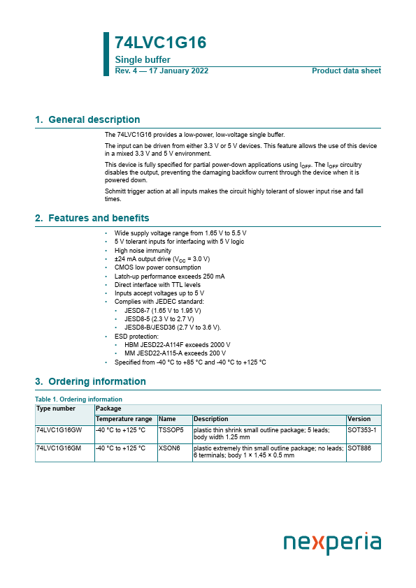
74LVC1G16 Single buffer Rev. 4 — 17 January 2022 Product data sheet 1. General description The 74LVC1G16 provides a low-power, low-voltage single buffer. The input can be driven from either 3.3 V or 5 V devices. This feature allows the use of this device in a mixed 3.3 V and 5 V environment. This device is fully specified for partial power-down applications using IOFF. The IOFF circuitry disables the output, preventing the damaging backflow current through the device when it is powered down. Schmitt trigger action at all inputs makes the circuit highly tolerant of slower input rise and fall times. 2. Features and benefits • Wide supply voltage range from 1.65 V to 5.5 V • 5 V tolerant inputs for interfacing with 5 V logic • High noise immunity • ±24 mA output drive (VCC = 3.
Published: |