Datasheet4U Logo Datasheet4U.com
Nexperia logo

74LVC2G74

Manufacturer: Nexperia

74LVC2G74 datasheet by Nexperia.

74LVC2G74 datasheet preview

74LVC2G74 Datasheet Details

Part number 74LVC2G74
Datasheet 74LVC2G74-nexperia.pdf
File Size 273.37 KB
Manufacturer Nexperia
Description Single D-type flip-flop
74LVC2G74 page 2 74LVC2G74 page 3

74LVC2G74 Overview

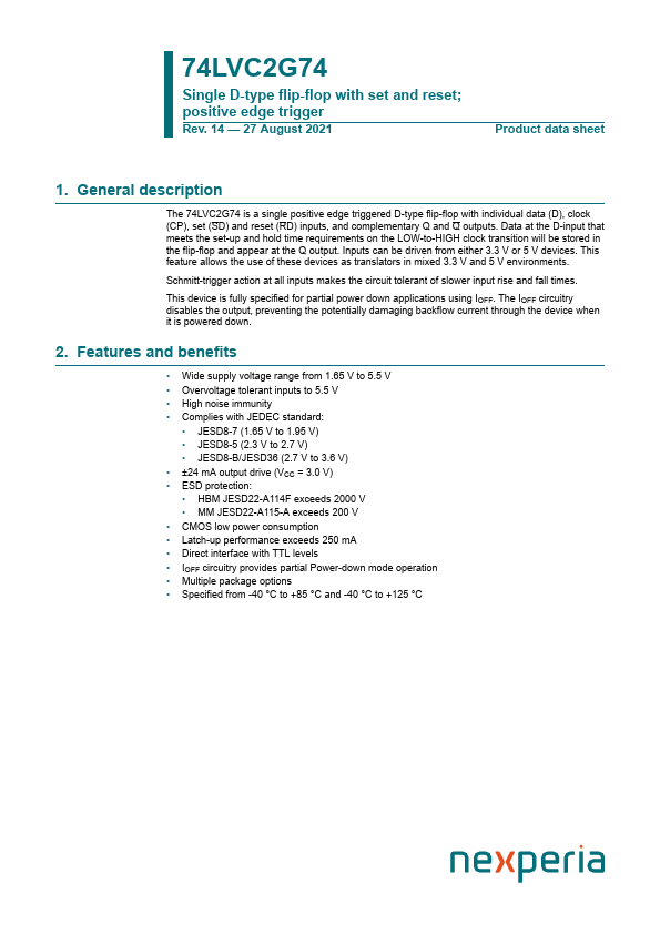
The 74LVC2G74 is a single positive edge triggered D-type flip-flop with individual data (D), clock (CP), set (SD) and reset (RD) inputs, and plementary Q and Q outputs. Data at the D-input that meets the set-up and hold time requirements on the LOW-to-HIGH clock transition will be stored in the flip-flop and appear at the Q output. Inputs can be driven from either 3.3 V or 5 V devices.

74LVC2G74 Key Features

  • Wide supply voltage range from 1.65 V to 5.5 V
  • Overvoltage tolerant inputs to 5.5 V
  • High noise immunity
  • plies with JEDEC standard
  • JESD8-7 (1.65 V to 1.95 V)
  • JESD8-5 (2.3 V to 2.7 V)
  • JESD8-B/JESD36 (2.7 V to 3.6 V)
  • ±24 mA output drive (VCC = 3.0 V)
  • ESD protection
  • HBM JESD22-A114F exceeds 2000 V

74LVC2G74 Applications

  • Wide supply voltage range from 1.65 V to 5.5 V
  • Overvoltage tolerant inputs to 5.5 V

74LVC2G74 from other manufacturers

View 74LVC2G74 datasheet index

Brand Logo Part Number Description Other Manufacturers
NXP Semiconductors Logo 74LVC2G74 Single D-type flip-flop NXP Semiconductors
Nexperia logo - Manufacturer

More Datasheets from Nexperia

View all Nexperia datasheets

Part Number Description
74LVC2G74-Q100 Single D-type flip-flop
74LVC2G00 Dual 2-input NAND gate
74LVC2G00-Q100 Dual 2-input NAND gate
74LVC2G02 Dual 2-input NOR gate
74LVC2G02-Q100 Dual 2-input NOR gate
74LVC2G04 Dual inverter
74LVC2G04-Q100 Dual inverter
74LVC2G06 Inverters
74LVC2G06-Q100 Inverters
74LVC2G07 Buffers

74LVC2G74 Distributor

Datasheet4U Logo
Since 2006. D4U Semicon. About Datasheet4U Contact Us Privacy Policy Purchase of parts