Datasheet4U Logo Datasheet4U.com

74LVC594A - 8-bit shift register

Datasheet Summary

Description

The 74LVC594A is an 8-bit serial-in/serial or parallel-out shift register with a storage register.

Separate clock and reset inputs are provided on both shift and storage registers.

Features

  • Overvoltage tolerant inputs to 5.5 V.
  • Wide supply voltage range from 1.2 V to 3.6 V.
  • CMOS low power dissipation.
  • Direct interface with TTL levels.
  • IOFF circuitry provides partial Power-down mode operation.
  • Balanced propagation delays.
  • All inputs have Schmitt-trigger action.
  • Complies with JEDEC standard:.
  • JESD8-7A (1.65 V to 1.95 V).
  • JESD8-5A (2.3 V to 2.7 V).
  • JESD8-C/JESD36 (2.7 V to 3.6 V).

📥 Download Datasheet

Datasheet preview – 74LVC594A

Datasheet Details

Part number 74LVC594A
Manufacturer nexperia
File Size 281.56 KB
Description 8-bit shift register
Datasheet download datasheet 74LVC594A Datasheet
Additional preview pages of the 74LVC594A datasheet.
Other Datasheets by nexperia

Full PDF Text Transcription

Click to expand full text
74LVC594A 8-bit shift register with output register Rev. 4 — 3 September 2020 Product data sheet 
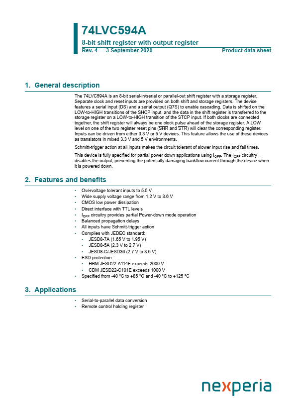
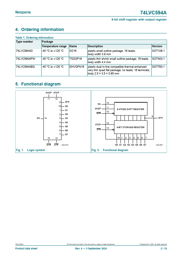
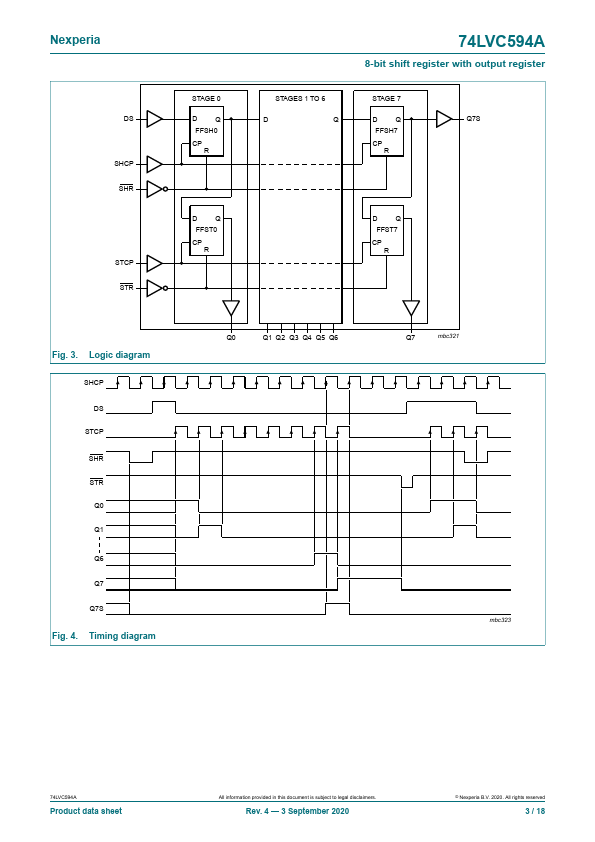
1. General description The 74LVC594A is an 8-bit serial-in/serial or parallel-out shift register with a storage register. Separate clock and reset inputs are provided on both shift and storage registers. The device features a serial input (DS) and a serial output (Q7S) to enable cascading. Data is shifted on the LOW-to-HIGH transitions of the SHCP input, and the data in the shift register is transferred to the storage register on a LOW-to-HIGH transition of the STCP input. If both clocks are connected together, the shift register will always be one clock pulse ahead of the storage register. A LOW level on one of the two register reset pins (SHR and STR) will clear the corresponding register.
Published: |