Nexperia PMXB360ENEA
N-Channel MOSFET
| Part No. | PMXB360ENEA |
|---|---|
| Datasheet | PMXB360ENEA Download |
| Manufacturer |  Nexperia |
| Description | N-Channel MOSFET |
| Buy | Stock & Price |
FEATURES AND BENEFITS
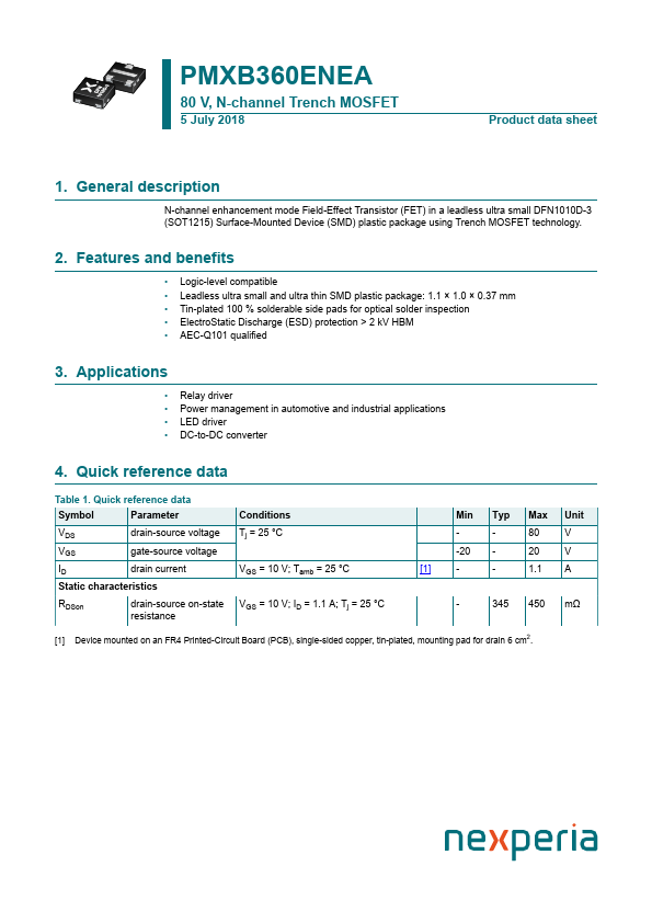
● Logic-level compatible● Leadless ultra small and ultra thin SMD plastic package: 1.1 × 1.0 × 0.37 mm
● Tin-plated 100 % solderable side pads for optical solder inspection
● ElectroStatic Discharge (ESD) protection > 2 kV HBM
● AEC-Q101 qualified 3.
APPLICATIONS
● Relay driver● Power management in automotive and industrial applications
● LED driver
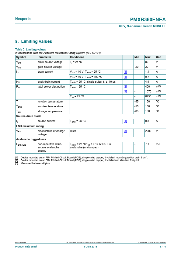
● DC-to-DC converter 4. Quick reference data Table 1. Quick reference data Symbol Parameter VDS drain-source voltage VGS gate-source voltage ID drain current Static characteristics RDSon drain-source on-state resistance Conditions Tj = 25 °C VGS = 10 V; Tamb = 25 °C VGS = 10 V; ID = 1.1 A; Tj = 25 °C Min Typ Max - - 80 -20 - 20 [1] - - 1.1 - 345 450 [1] Device mounted on an FR4 Printed-Circuit Board (PCB), single-sided copper, tin-plated, mounting pad for drain 6 cm2. Unit V V A mΩ Nexperia PMXB360ENEA 80 V, N-channel Trench MOSFET 5. Pinning information Table 2. Pinning information Pin Symbol
DESCRIPTION
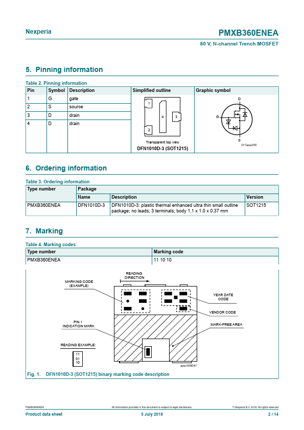
1 G gate 2 S source 3 D drain 4 D drain Simplified outline 1 Graphic symbol D 43 G 2 Transparent top view DFN1010D-3 (SOT1215) S 017aaa255 6.